SCDA008C June 2021 – November 2021 CD4052B , TS3A225E , TS3A44159
- Trademarks
- 1Introduction
- 2Semiconductor Switches
- 3Basic Signal-Switch Structures
- 4Key Concerns in Digital-Switch Applications
- 5Signal Switch Families
- 6Applications
- 7Conclusion
- 8References
- 9Revision History
-
A Test
Measurement Circuits
- A.1 Measurement Setup for ron
- A.2 Measurement Setup for VO vs VI Characteristics
- A.3 Voltage-Time Waveform Measurement (Switch On)
- A.4 Voltage-Time Waveform Measurement (Switch Off)
- A.5 Output-Skew Measurement
- A.6 Simulation Setup for Undershoot Measurement
- A.7 Laboratory Setup for Attenuation Measurement
- A.8 Laboratory Setup for Off Isolation Measurement
- A.9 Laboratory Setup for Crosstalk Measurement
4.11 Voltage Translation
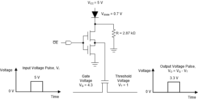
One popular application of the bus switch is voltage translation in a mixed-voltage environment. A simple NMOS can pass a signal from 0 V to VCC– VT, where VT is the threshold voltage of the NMOS. This characteristic can be used for down translation. Figure 4-4 shows an example of 5-V to 3.3-V translation using an NMOS series switch, diode, and resistors.
 Figure 4-4 Voltage Translation Using an
NMOS Series Switch
Figure 4-4 Voltage Translation Using an
NMOS Series SwitchFor voltage-translation applications, the switch is required to translate efficiently over a wide frequency range and is required to maintain the proper signal level. For example, when translating from a 5-V TTL to a 3.3-V LVTTL signal, the switch is required to maintain the required VOH (output high voltage) and VOL (output low voltage) of 3.3-V LVT TL signal. One important consideration is that the bus switch can be used only for down translation, for example, high to low-level. For low to high-level translation, additional components (for example, pullup resistors) are required.