SCDA039 October 2021 TMUX7308F , TMUX7309F , TMUX7412F , TMUX7462F
2 Multiplexer and Signal Switch Protection Against Fault Events
With all of these possibilities on the table, what can be done about it? The severity of these overvoltage and overstress events can cause real issues in many systems, however, TI offers a variety of multiplexers and signal switches that offer several built-in features that can protect against such events.
Overvoltage Fault Protection
One of the more common faults a system can experience is an Overvoltage Fault. Often caused from either a transient event, unstable power-up or power-down sequence, or a miswiring, this must to be given thorough consideration for every system. Fortunately, TI offers multiplexers and signal switches that include internal overvoltage protection circuitry that can handle such events.
As shown in Table 2-1 the Overvoltage Protection for these devices include the following features.
| Feature | Description |
|---|---|
| +/-60 V Overvoltage Protection | +/-60 V overvoltage protection in reference to ground |
| 85 V Absolute Maximum Voltage Across Pins | 85 V Between Source Pins and Supply Rails 85 V Between Source and Drain Pins |
| Overvoltage Programming | VFP and VFN pins that can be individually set to trip at a specific fault voltage. |
| Overvoltage Detection | When an overvoltage event is detected (VSource > VFP/VFN + VT OR VSource >VDD/VSS + VT), the channel experiencing the overvoltage event turns off and the Fault Flags (available on select devices) are set |
While these attributes are common across TI’s fault protected multiplexer family, each device implements these features slightly differently. Table 2-2 highlights some of these key differences and it is important to understand which would be best in each specific system.
| Device | Configuration | Fault Behavior | ||
|---|---|---|---|---|
| Trigger Supplies | Output Behavior | Flag | ||
| TMUX7308F/TMUX7309F | 8:1x1/4:1x2 | Primary (VDD/VSS) | Pull to Primary Supply | None |
| TMUX7411F/7412F/7413F | 1:1x4 | Primary (VDD/VSS) | Pull to Primary Supply | FF |
| TMUX7462F | 1:1x4 | Fault (VFP/VFN) | Pull to Fault Supply/Open | FF |
Depending on the desired system performance, designers will need to determine how they would like to have the multiplexer handle the fault events. The TMUX7308F represents a subset of devices where it offers the most generic protection as it has the overvoltage detection set at anything above the given supply rail. For more control, devices similar to the TMUX7462F allows the designer to control exactly where they would like to have the multiplexer trip for an overvoltage event. The system examples Figure 2-1 and Figure 2-2 illustrate how to use these devices in different situations:
When the downstream devices need to be protected to the same level as the fault protected multiplexer, the TMUX7308F is a sufficient solution here as it will protect up to the VDD/VSS rail voltage. If there is a need to customize the fault protected mux to protect against a certain threshold, the TMUX7462F allows the designer to set the exact trip voltage using the VFP/VFN pins in order to prevent downstream damage.
Other important considerations include the reporting of faults (using fault flag pins SF and FF) which is offered on some multiplexers and also the output behavior demonstrated when there is a fault. The output can be put into an open state or can be pulled to a supply rail. The TMUX7462F is unique as it has an addition DR (drain response) pin that lets the user dictate how to operate the state of the output during a fault event. If the DR pin is pulled low, it will be pulled to the supply that is exceeded. However, if pulled high or floated, it will become high impedance.
The fault flags, SF (Specific Fault Flag) and FF (General Fault Flag) are often used in conjunction with a microcontroller to help report system faults. Both of these pins are open drain outputs and are asserted low when the multiplexer detects an event occurred. When the event occurs, the FF pin will be pulled low and report that one of the device inputs has encountered a fault. The SF pin, however, will be asserted low only when the fault affected channel is selected with the address pins. Like mentioned previously, some devices may either have one, both, or neither of these pins.
Powered-Off Protection
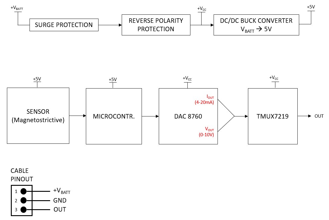
Another critical feature of these protection multiplexers it their inherent Powered-Off protection circuitry which allows the devices to sustain overvoltage events of up to +/-60V when the supplies are removed or at 0V. This provides relief from power sequencing difficulties as well as miswiring instances. Take the system Figure 2-5 shown as an example of all the possible miswiring combinations with just three inputs and the repercussions on the TMUX7219 device:
 Figure 2-5 Miswiring on a Non-Fault Protected Device
| Combinations | Result | ||
|---|---|---|---|
| VCC | D | GND | |
| VBATT | OUT | GND | Operates without issue |
| VBATT | GND | OUT | GND pin/circuit is now floating or at the potential the OUT cable is connected to. This could be a problem depending what is on that side of the OUT cable. Remainder of circuit is OK. |
| OUT | VBATT | GND | VCC is now floating or at the potential the OUT cable is at. VBATT is now attached to the input and most likely at a higher potential than VCC, thus turning on the ESD protection diode and possibly back powering device |
| OUT | GND | VBATT | VCC is now floating or at the potential the OUT cable is at. VBATT is now attached to the GND and the input most likely has a lower potential than VBATT, thus turning on the ESD protection diode and causing current to flow, possibly damaging the device if no current limiting resistor is in place. |
| GND | VBATT | OUT | VCC is now grounded. GND is floating or at potential of OUT cable. Input is at VBATT which will cause the ESD diode to turn on and possibly back power the device. |
| GND | OUT | VBATT | VCC is now grounded. GND is at VBATT and input is floating or at potential of OUT cable. S pin voltage will be lower than GND, thus turning on ESD protection diode and allowing current to flow. Could cause damage if current is too high. Need current limiting resistor |
Essentially, all of the situations except the correct wiring will pose some risk to the device and system if there is no implementation of a protection device that does not incorporate powered off protection. With this feature, all of these combinations are accounted for and can be protected against.
Current Limit Protection
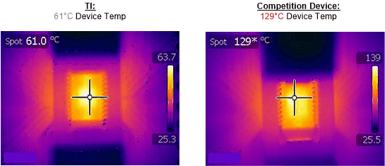
While there are many sources that can cause an overvoltage event, the system also needs to take into consideration the possibility of an overcurrent event. The TI Fault Protection Multiplexer family has a unique architecture to help limit the current to a fixed amount while also keeping the device within its maximum junction temperature. Figure 2-6 is an example of TI versus a competitor device under the same shorted fault condition at 25C:
 Figure 2-6 TI Device vs. Competitor Device
As the temperature is increased to 125C, the TI device under fault increases to 145°C which is still within the absolute maximum junction temperature of 150°C while the competition device can get up to 200°C. An important note is that these devices are not meant to be left in this shorted state indefinitely and the fault should be cleared as soon as possible. For information on the approximate current limit for each fault protected device, it can be estimated from the IDC parameter defined in each data sheet at the specified temperature.
Integrated vs. Discrete Solution
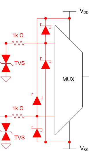
Even though some of these overvoltage and overstress situations can be addressed using external components, there are often significant drawbacks when doing so. Figure 2-7 is an illustration of the extra components that would be needed to replicate only some of the features boasted by the TI Fault Protected Multiplexer family.
 Figure 2-7 Mux without Integrated Fault Protection
TVS diodes on every input, Schottky or Zener diodes between the supply rails and the input, and current limiting resistors would be required to do just a subset of what the integrated solution can do. In addition, the system level repercussions are significant when implementing a discrete solution:
| Discrete Protection Drawback | System Level Impact |
|---|---|
| Series resistor increases the settling time of the signal | Limits switching speed of the multiplexer and slows down the system |
| Protection diodes introduce additional leakage current and parasitic capacitance | Impact system measurement accuracy and affect linearity |
| No protection in floating supply case | Impact system robustness during uncontrolled power sequencing events |
| Large number of components required | Add system cost and increase board size |