SCDS404B March 2021 – November 2022 TMUX7411F , TMUX7412F , TMUX7413F
PRODMIX
- 1 Features
- 2 Applications
- 3 Description
- 4 Revision History
- 5 Device Comparison Table
- 6 Pin Configuration and Functions
-
7 Specifications
- 7.1 Absolute Maximum Ratings
- 7.2 ESD Ratings
- 7.3 Thermal Information
- 7.4 Recommended Operating Conditions
- 7.5 Electrical Characteristics: Global
- 7.6 ±15 V Dual Supply: Electrical Characteristics
- 7.7 ±20 V Dual Supply: Electrical Characteristics
- 7.8 12 V Single Supply: Electrical Characteristics
- 7.9 36 V Single Supply: Electrical Characteristics
- 7.10 Typical Characteristics
-
8 Parameter Measurement Information
- 8.1 On-Resistance
- 8.2 Turn-On and Turn-Off Time
- 8.3 Off-Leakage Current
- 8.4 On-Leakage Current
- 8.5 Input and Output Leakage Current Under Overvoltage Fault
- 8.6 Fault Response Time
- 8.7 Fault Recovery Time
- 8.8 Fault Flag Response Time
- 8.9 Fault Flag Recovery Time
- 8.10 Charge Injection
- 8.11 Off Isolation
- 8.12 Inter-Channel Crosstalk
- 8.13 Bandwidth
- 8.14 THD + Noise
- 9 Detailed Description
- 10Application and Implementation
- 11Power Supply Recommendations
- 12Layout
- 13Device and Documentation Support
- 14Mechanical, Packaging, and Orderable Information
3 Description
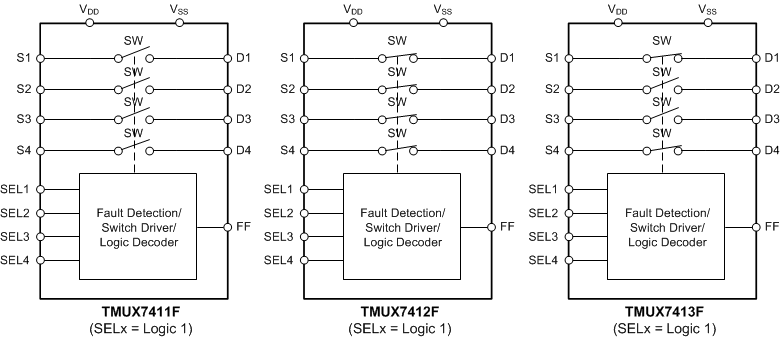
The TMUX7411F, TMUX7412F, and TMUX7413F are complementary metal-oxide semiconductor (CMOS) analog switches in 1:1 (SPST), 4-channel configurations. The devices work well with dual supplies (±5 V to ±22 V), a single supply (8 V to 44 V), or asymmetric supplies (such as VDD = 12 V, VSS = –5 V). The overvoltage protection is available in powered and powered-off conditions, making the TMUX741xF devices suitable for applications where power supply sequencing cannot be precisely controlled.
The devices block fault voltages up to +60 V or
−60 V relative to ground in powered and powered-off
conditions. When no power supplies are present, the switch channels remain in the
OFF state regardless of the switch input conditions, and any control signal present
on the logic pins is ignored. If the signal path input voltage on any Sx pin exceeds
the supply voltage (VDD or VSS) by a threshold voltage
(VT), the channel turns OFF and the Sx pin becomes high impedance.
The drain pin (Dx) of a selected channel under a fault condition is floating. The
TMUX741xF devices provide an active-low interrupt flag (FF) to indicate if any of
the source inputs are experiencing a fault condition to help system diagnostics.
| PART NUMBER | PACKAGE | BODY SIZE (NOM) |
|---|---|---|
| TMUX7411F TMUX7412F TMUX7413F | PW (TSSOP, 16) (2) | 5.00 mm × 4.40 mm |
| RRP (WQFN, 16) | 4.00 mm × 4.00 mm |
 Functional Block Diagram