SCDS418F July 2020 – July 2024 TMUX7208 , TMUX7209
PRODUCTION DATA
- 1
- 1 Features
- 2 Applications
- 3 Description
- 4 Device Comparison Table
- 5 Pin Configuration and Functions
-
6 Specifications
- 6.1 Absolute Maximum Ratings
- 6.2 ESD Ratings
- 6.3 Thermal Information
- 6.4 Recommended Operating Conditions
- 6.5 Source or Drain Continuous Current
- 6.6 ±15 V Dual Supply: Electrical Characteristics
- 6.7 ±15 V Dual Supply: Switching Characteristics
- 6.8 ±20 V Dual Supply: Electrical Characteristics
- 6.9 ±20 V Dual Supply: Switching Characteristics
- 6.10 44 V Single Supply: Electrical Characteristics
- 6.11 44 V Single Supply: Switching Characteristics
- 6.12 12 V Single Supply: Electrical Characteristics
- 6.13 12 V Single Supply: Switching Characteristics
- 6.14 Typical Characteristics
-
7 Parameter Measurement Information
- 7.1 On-Resistance
- 7.2 Off-Leakage Current
- 7.3 On-Leakage Current
- 7.4 Transition Time
- 7.5 tON(EN) and tOFF(EN)
- 7.6 Break-Before-Make
- 7.7 tON (VDD) Time
- 7.8 Propagation Delay
- 7.9 Charge Injection
- 7.10 Off Isolation
- 7.11 Crosstalk
- 7.12 Bandwidth
- 7.13 THD + Noise
- 7.14 Power Supply Rejection Ratio (PSRR)
- 8 Detailed Description
- 9 Application and Implementation
- 10Device and Documentation Support
- 11Revision History
- 12Mechanical, Packaging, and Orderable Information
3 Description
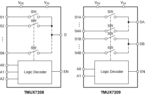
The TMUX7208 is a precision 8:1, single channel multiplexer while the TMUX7209 is a 4:1, 2 channel multiplexer featuring low on resistance and charge injection. The devices work with a single supply (4.5V to 44V), dual supplies (±4.5V to ±22V), or asymmetric supplies (such as VDD = 12V, VSS = –5V). The TMUX720x support bidirectional analog and digital signals on the source (Sx) and drain (D) pins ranging from VSS to VDD.
The TMUX720x are part of the precision switches and multiplexers family of devices and have very low on and off leakage currents allowing them to be used in high precision measurement applications. The TMUX720x family provides latch-up immunity, preventing undesirable high current events between parasitic structures within the device typically caused by overvoltage events. A latch-up condition typically continues until the power supply rails are turned off and can lead to device failure. The latch-up immunity feature allows the TMUX720x family of switches and multiplexers to be used in harsh environments.
| PART NUMBER (1) | CONFIGURATION | PACKAGE(2) |
|---|---|---|
| TMUX7208 | 1 Channel 8:1 Multiplexer |
PW (TSSOP, 16) |
| TMUX7209 | 2 Channel 4:1 Multiplexer |
RUM (WQFN, 16) |
 TMUX7208 and TMUX7209 Block Diagram