SCDS418F July 2020 – July 2024 TMUX7208 , TMUX7209
PRODUCTION DATA
- 1
- 1 Features
- 2 Applications
- 3 Description
- 4 Device Comparison Table
- 5 Pin Configuration and Functions
-
6 Specifications
- 6.1 Absolute Maximum Ratings
- 6.2 ESD Ratings
- 6.3 Thermal Information
- 6.4 Recommended Operating Conditions
- 6.5 Source or Drain Continuous Current
- 6.6 ±15 V Dual Supply: Electrical Characteristics
- 6.7 ±15 V Dual Supply: Switching Characteristics
- 6.8 ±20 V Dual Supply: Electrical Characteristics
- 6.9 ±20 V Dual Supply: Switching Characteristics
- 6.10 44 V Single Supply: Electrical Characteristics
- 6.11 44 V Single Supply: Switching Characteristics
- 6.12 12 V Single Supply: Electrical Characteristics
- 6.13 12 V Single Supply: Switching Characteristics
- 6.14 Typical Characteristics
-
7 Parameter Measurement Information
- 7.1 On-Resistance
- 7.2 Off-Leakage Current
- 7.3 On-Leakage Current
- 7.4 Transition Time
- 7.5 tON(EN) and tOFF(EN)
- 7.6 Break-Before-Make
- 7.7 tON (VDD) Time
- 7.8 Propagation Delay
- 7.9 Charge Injection
- 7.10 Off Isolation
- 7.11 Crosstalk
- 7.12 Bandwidth
- 7.13 THD + Noise
- 7.14 Power Supply Rejection Ratio (PSRR)
- 8 Detailed Description
- 9 Application and Implementation
- 10Device and Documentation Support
- 11Revision History
- 12Mechanical, Packaging, and Orderable Information
7.14 Power Supply Rejection Ratio (PSRR)
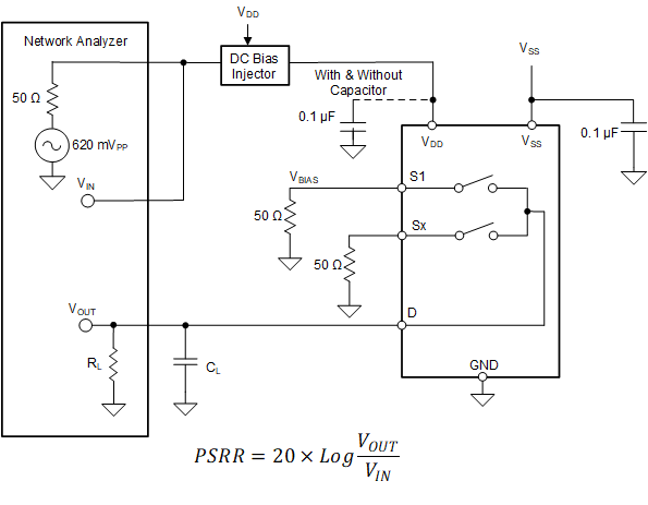
PSRR measures the ability of a device to prevent noise and spurious signals that appear on the supply voltage pin from coupling to the output of the switch. The DC voltage on the device supply is modulated by a sine wave of 620mVPP. The ratio of the amplitude of signal on the output to the amplitude of the modulated signal is the ACPSRR. A high ratio represents a high degree of tolerance to supply rail variation.
The below shows how the decoupling capacitors reduce high frequency noise on the supply pins. This helps stabilize the supply and immediately filter as much of the supply noise as possible.
 Figure 7-14 ACPSRR
Measurement Setup