SCEA064A June 2019 – March 2021 2N7001T , SN74AXC4T245 , SN74AXC4T774 , TXB0104
5 Joint Test Access Group (JTAG)
The Joint Test Access Group developed a hardware interface to allow for the debugging, programming, and testing of embedded devices. JTAG, similar to SPI, operates using a set of five JTAG interface signals as shown in Table 5-1.
| SIGNAL | DESCRIPTION | DIRECTION |
|---|---|---|
| TCK | Test Clock Signal | Controller to Debugger |
| TDI | Test Data In | Controller to Debugger |
| TDO | Test Data Out | Debugger to Controller |
| TMS | Test Mode Select | Controller to Debugger |
| TRST (Optional) | Test Reset | Controller to Debugger |
The test clock is used to provide a steady timing signal at which the test data will arrive. The test mode select allows the user to select what section or circuit is going to be tested. The JTAG protocol depends on the device being tested. TDI is the pin that is used to perform the test and the results are returned through the TDO pin. The optional test reset pin allows the ability to reset JTAG to a known good state.
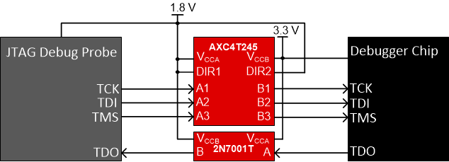
Usually, there are multiple devices on a board that need to be tested via the JTAG interface. Using JTAG, these devices can be daisy chained to each other with the TDO pin, which extends out of the last device in the chain. If this last device in the daisy chain is on a different voltage level, the 2N7001T can be used for a voltage translation. The signal flow of TDO is opposite to the direction of the other pins allowing for the use of the 2N7001T in combination with SN74AXC4T245, for the remaining three channels.
 Figure 5-1 JTAG Interface Using 2N7001T Device