SCES959A December 2023 – April 2024 TXV0108
PRODUCTION DATA
- 1
- 1 Features
- 2 Applications
- 3 Description
- 4 Pin Configuration and Functions
-
5 Specifications
- 5.1 Absolute Maximum Ratings
- 5.2 ESD Ratings
- 5.3 Recommended Operating Conditions
- 5.4 Thermal Information
- 5.5 Electrical Characteristics
- 5.6 Switching Characteristics, VCCA = 1.2 ± 0.06 V
- 5.7 Switching Characteristics, VCCA = 1.8 ± 0.15 V
- 5.8 Switching Characteristics, VCCA = 2.5 ± 0.2 V
- 5.9 Switching Characteristics, VCCA = 3.3 ± 0.3 V
- 5.10 Typical Characteristics
- 6 Parameter Measurement Information
-
7 Detailed Description
- 7.1 Overview
- 7.2 Functional Block Diagram
- 7.3
Feature Description
- 7.3.1 Balanced High-Drive CMOS Push-Pull Outputs
- 7.3.2 Partial Power Down (Ioff)
- 7.3.3 VCC Isolation and VCC Disconnect (Ioff-float)
- 7.3.4 Over-Voltage Tolerant Inputs
- 7.3.5 Negative Clamping Diodes
- 7.3.6 Fully Configurable Dual-Rail Design
- 7.3.7 Supports Timing Sensitive Translation
- 7.3.8 Integrated Damping Resistor and Impedance Matching
- 7.4 Device Functional Modes
- 8 Application and Implementation
- 9 Device and Documentation Support
- 10Revision History
- 11Mechanical, Packaging, and Orderable Information
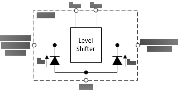
7.3.5 Negative Clamping Diodes
The inputs and outputs to this device have negative clamping diodes as shown in Figure 7-3
CAUTION:
Voltages beyond the values specified in the Absolute Maximum Ratings table can cause damage to the device. The input negative-voltage and output voltage ratings may be exceeded if the input and output clamp-current ratings are observed.
 Figure 7-3 Electrical Placement of
Clamping Diodes for Each Input and Output