SCEU031B August   2024  – October 2024 TPLD801

PRODUCTION DATA  

  1.   1
  2.   Description
  3.   Get Started
  4.   Features
  5.   Applications
  6.   6
  7. 1Evaluation Module Overview
    1. 1.1 Introduction
    2. 1.2 Kit Contents
    3. 1.3 Specification
    4. 1.4 Device Information
  8. 2Hardware
    1. 2.1 Functional Blocks
      1. 2.1.1 Test Points
      2. 2.1.2 Programmer Header Block (P1)
      3. 2.1.3 External Connection Header Block
      4. 2.1.4 GPI Protection Block
      5. 2.1.5 DRL Socket
      6. 2.1.6 SW or LED Testing Blocks
      7. 2.1.7 GPI Switch Testing Block
  9. 3Software
    1. 3.1 Using the TPLD801-DRL-EVM
      1. 3.1.1 Equipment Needed for Programming
      2. 3.1.2 Installing Software
    2. 3.2 Configuring a TPLD Device
      1. 3.2.1 TPLD801-DRL-EVM Setup for Programming
      2. 3.2.2 Inserting a TPLD801DRL into the DRL Socket
      3. 3.2.3 Connecting the TPLD801-DRL-EVM to a TPLD-PROGRAM Board
      4. 3.2.4 Temporarily Configuring a TPLD Device
      5. 3.2.5 Permanently Programming a TPLD Device
  10. 4Hardware Design Files
    1. 4.1 Schematics
    2. 4.2 PCB Layout
      1. 4.2.1 PCB Overview
    3. 4.3 Bill of Materials
  11. 5Additional Information
    1. 5.1 Trademarks
  12. 6Revision History

GPI Switch Testing Block

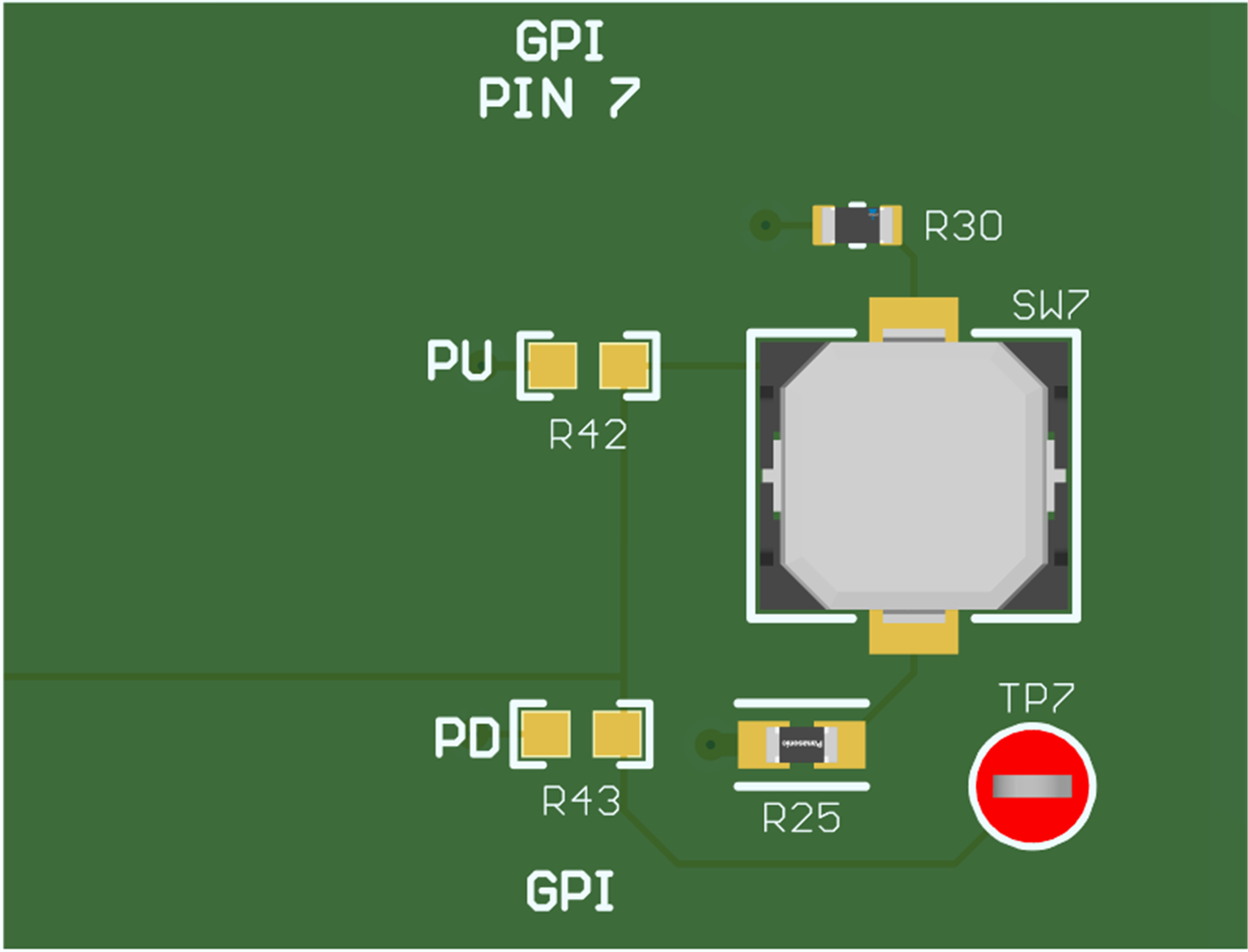
The GPI line is connected to a tactile switch. This switch has no debounce features. This is to protect the GPI signal during programming. The GPU switch block has soldering spots for optional pull-up and pull-down resistors. These are initially de-populated and are labeled PU and PD, respectively. Do not attempt to permanently program the device with either a pull-up or pull-down resistor installed on the GPI line.
TPLD801-DRL-EVM GPI Switch Block Figure 2-4 GPI Switch Block