SCLS737E September 2013 – July 2024 SN74LV1T00
PRODUCTION DATA
- 1
- 1 Features
- 2 Applications
- 3 Description
- 4 Related Products
- 5 Pin Configuration and Functions
- 6 Specifications
- 7 Parameter Measurement Information
- 8 Detailed Description
- 9 Application and Implementation
- 10Device and Documentation Support
- 11Revision History
- 12Mechanical, Packaging, and Orderable Information
3 Description
SN74LV1T00 is a low voltage CMOS gate logic that operates at a wider voltage range for industrial, portable, telecom, and automotive applications. The output level is referenced to the supply voltage and is able to support 1.8V/2.5V/3.3V/5V CMOS levels
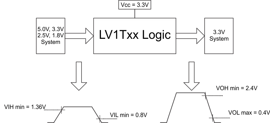
The input is designed with a lower threshold circuit to match 1.8V input logic at VCC = 3.3V and can be used in 1.8V to 3.3V level up translation. In addition, the 5V tolerant input pins enable down translation (e.g. 3.3V to 2.5V output at VCC = 2.5V). The wide VCC range of 1.8V to 5.5V allows generation of desired output levels to connect to controllers or processors.
The SN74LV1T00 is designed with current-drive capability of 8 mA to reduce line reflections, overshoot, and undershoot caused by high-drive outputs.
| DEVICE NUMBER | PACKAGE(1) | PACKAGE SIZE(2) | BODY SIZE(3) |
|---|---|---|---|
| SN74LV1T00 | DBV (SOT-23, 5) | 2.9mm x 2.8mm | 2.9mm x 1.6mm |
| DCK (SC-70, 5) | 2mm x 2.1mm | 2mm x 1.25mm |
 Switching Thresholds for 1.8V to 3.3V Translation