SFFS521A September 2022 – November 2024 LM5168 , LM5169
4 Pin Failure Mode Analysis (Pin FMA)
This section provides a failure mode analysis (FMA) for the pins of the LM5168 and LM5169. The failure modes covered in this document include the typical pin-by-pin failure scenarios:
- Pin short-circuited to ground (see Table 4-2)
- Pin open-circuited (see Table 4-3)
- Pin short-circuited to an adjacent pin (see Table 4-4)
- Pin short-circuited to VIN (see Table 4-5)
Table 4-2 through Table 4-5 also indicate how these pin conditions can affect the device as per the failure effects classification in Table 4-1.
| Class | Failure Effects |
|---|---|
| A | Potential device damage that affects functionality. |
| B | No device damage, but loss of functionality. |
| C | No device damage, but performance degradation. |
| D | No device damage, no impact to functionality or performance. |
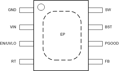
Figure 4-1 and Figure 4-2 show the LM5168 and LM5169 pin diagrams for the HSOIC and WSON packages, respectively. For a detailed description of the device pins, see the Pin Configuration and Functions section in the LM5168 and LM5169 data sheets.
 Figure 4-1 Pin Diagram for HSOIC
  Figure 4-2 Pin Diagram for WSON
Following are the assumptions of use and the device configuration assumed for the pin FMA in this section:
- Device used within the Recommended Operating Conditions and the Absolute Maximum Ratings found in LM5169, LM5168 0.65-A/0.3-A, 120-V, Step-Down Converter with Fly-Buck™ Converter Capability Data Sheet
- Configuration as shown in the Example Application Circuit found in the LM5169, LM5168 0.65-A/0.3-A, 120-V, Step-Down Converter with Fly-Buck™ Converter Capability Data Sheet.
- Valid for an ambient temperature of 25°C.
- Faults applied after device start-up is complete.
| Pin Name | Pin No. | Description of Potential Failure Effects | Failure Effect Class |
|---|---|---|---|
| GND | 1 | Normal operation. | D |
| VIN | 2 | Input supply shorted to ground. No output voltage. | B |
| EN/UVLO | 3 | No output voltage. Loss of EN/UVLO functionality. | B |
| RT | 4 | No or low output voltage. | B |
| FB | 5 | Output voltage increases to near input voltage level. Possible damage to load. | B |
| PGOOD | 6 | Normal operation. Loss of PGOOD function. | B |
| BST | 7 | No output voltage. Possible device damage. | A |
| SW | 8 | No output voltage. Possible device damage. | A |
| Pin Name | Pin No. | Description of Potential Failure Effects | Failure Effect Class |
|---|---|---|---|
| GND | 1 | No output voltage. | B |
| VIN | 2 | No output voltage. | B |
| EN/UVLO | 3 | No output voltage. Loss of EN/UVLO functionality. | B |
| RT | 4 | Output voltage out of regulation. Possible damage to load. | B |
| FB | 5 | Output voltage out of regulation. Possible damage to load. | B |
| PGOOD | 6 | Normal operation. Loss of PGOOD function. | B |
| BST | 7 | No output voltage. | B |
| SW | 8 | No output voltage. | B |
| Pin Name | Pin No. | Shorted to | Description of Potential Failure Effects | Failure Effect Class |
|---|---|---|---|---|
| GND | 1 | 2, VIN | No output voltage. Input supply shorted to ground. | B |
| VIN | 2 | 3, EN/UVLO | Normal operation. Loss of EN/UVLO functionality. | B |
| EN/UVLO | 3 | 4, RT | No output voltage. Possible device damage. | A |
| FB | 5 | 6, PGOOD | Output voltage out of regulation. Possible damage to load. | B |
| PGOOD | 6 | 7, BST | No output voltage. | B |
| BST | 7 | 8, SW | No output voltage. | B |
| Pin Name | Pin No. | Description of Potential Failure Effects | Failure Effect Class |
|---|---|---|---|
| GND | 1 | Input supply shorted. No output voltage. | B |
| VIN | 2 | Normal operation. | D |
| EN/UVLO | 3 | Normal operation. EN/UVLO functionality lost. | B |
| RT | 4 | No output voltage. Device damage. | A |
| FB | 5 | No output voltage. Device damage. | A |
| PGOOD | 6 | Loss of PGOOD functionality. Possible device damage. | A |
| BST | 7 | No output voltage. Device damage. | A |
| SW | 8 | Output voltage at level of input voltage. Damage to load. Possible device damage. | A |