SFFS689 December 2023 TPS2663
4.1 VQFN Package
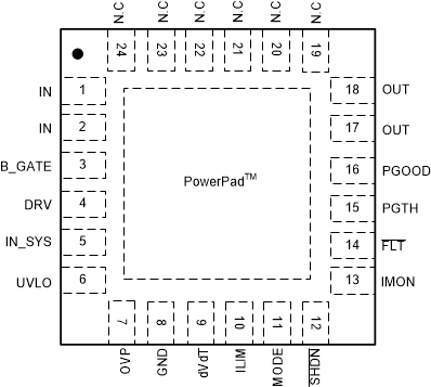
Figure 4-1 shows the TPS2663 pin diagram for the VQFN package. For a detailed description of the device pins please refer to the Pin Configuration and Functions section in the TPS2663 data sheet.
 Figure 4-1 TPS26630, TPS26631 Pin Diagram
(VQFN) Package
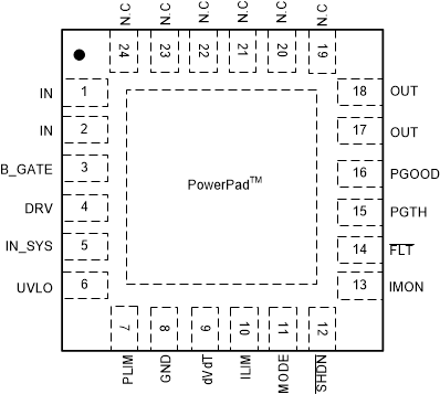
 Figure 4-2 TPS26632, TPS26633, TPS26635
Pin Diagram (VQFN) Package
Figure 4-2 TPS26632, TPS26633, TPS26635
Pin Diagram (VQFN) PackageTable 4-2 Pin FMA for Device Pins
Short-Circuited to Ground
| Pin Name | Pin No. | Description of Potential Failure Effect(s) | Failure Effect Class |
|---|---|---|---|
| IN | 1,2 | Device unpowered. Device not functional. | B |
| B_GATE | 3 | Potential device damage | A |
| DRV | 4 | Potential device damage | A |
| IN_SYS | 5 | Device unpowered. Device not functional. | B |
| UVLO | 6 | UVLO protection is triggered. Device turns off the internal FET. | B |
| OVP or PLIM | 7 | Over-voltage protection or power limiting does not function. | B |
| GND | 8 | No effect. Normal operation. | D |
| dVdT | 9 | Device does not power up. | B |
| ILIM | 10 | Device does not power up. | B |
| MODE | 11 | Device provides auto-retry behavior for over-current events as per device functional modes in data sheet. | D |
| SHDN | 12 | Device is disabled. | B |
| IMON | 13 | Current monitor function is not available. | B |
| FLT | 14 | Fault function is not available. | B |
| PGTH | 15 | PGOOD function is not available. | B |
| PGOOD | 16 | PGOOD function is not available. | B |
| OUT | 17, 18 | Device enters into current limiting operation. | B |
| NC | 19, 20, 21, 22, 23, 24 | No effect. Normal operation. | D |
Table 4-3 Pin FMA for Device Pins
Open-Circuited
| Pin Name | Pin No. | Description of Potential Failure Effect(s) | Failure Effect Class |
|---|---|---|---|
| IN | 1,2 | Device unpowered. Device is not functional. | B |
| B_GATE | 3 | Reverse current blocking and Reverse polarity protection are not functional. | B |
| DRV | 4 | Reverse current blocking and Reverse polarity protection are not functional. | B |
| IN_SYS | 5 | Device unpowered. Device is not functional. | B |
| UVLO | 6 | Device functionality undetermined. Device may turn off / power down. | B |
| OVP or PLIM | 7 | TPS26630, TPS26631: over-voltage protection function is not determined. Device may turn off the internal FET. TPS26632, TPS26633, TPS26635: output power limit is set to power more than 400 W. | B |
| GND | 8 | Device unpowered. Device is not functional. | B |
| dVdT | 9 | Device provides slew rate 24 V/500 μs on output. | D |
| ILIM | 10 | Internal FET is turned off. Output is not powered up. | B |
| MODE | 11 | Device provides latch-off behavior for over-current events as per device functional modes in data sheet. | D |
| SHDN | 12 | No effect. Normal operation. | D |
| IMON | 13 | No effect. Normal operation. | D |
| FLT | 14 | No effect. Normal operation. | D |
| PGTH | 15 | PGOOD might not function. | B |
| PGOOD | 16 | No effect. Normal operation. | D |
| OUT | 17, 18 | No power or current provided to load. | D |
| NC | 19, 20, 21, 22, 23, 24 | No effect. Normal operation. | D |
Table 4-4 Pin FMA for Device Pins
Short-Circuited to Adjacent Pin
| Pin Name | Pin No. | Description of Potential Failure Effect(s) | Failure Effect Class |
|---|---|---|---|
| IN | 1,2 | IN to B_GATE: Potential device damage | A |
| B_GATE | 3 | B_GATE to DRV : Potential device damage | A |
| DRV | 4 | DRV to IN_SYS : Potential device damage | A |
| IN_SYS | 5 | IN_SYS to UVLO: under-voltage protection does not function. | B |
| UVLO | 6 | UVLO to OVP/PLIM: potential device damage if UVLO voltage is more than 5.5 V. | A |
| OVP or PLIM | 7 | OVP/PLIM to GND: over-voltage protection or Power limiting does not function. | B |
| GND | 8 | GND to dVdT: device unpowered. Device not functional. | B |
| dVdT | 9 | dVdT to ILIM: device can go into current limit operation. | B |
| ILIM | 10 | ILIM to MODE: device can go into current limit operation or Latch-off mode. | B |
| MODE | 11 | MODE to SHDN: device can go into shutdown. | B |
| SHDN | 12 | SHDN to IMON: device can go into shutdown. | B |
| IMON | 13 | IMON to FLT: potential Device damage if FLT pin voltage is more than 5.5 V. | A |
| FLT | 14 | FLT to PGTH : PGOOD does not function if FLT is low. | B |
| PGTH | 15 | PGTH to PGOOD : PGOOD does not function | B |
| PGOOD | 16 | PGOOD to OUT: Potential device damage when PGOOD is low and output is powered up. | A |
| OUT | 17, 18 | OUT to N.C: no effect. Normal operation. | D |
| NC | 19, 20, 21, 22, 23, 24 | NC to IN short or NC to NC short : No effect. Normal operation. | D |
Table 4-5 Pin FMA for Device Pins Short-Circuited to IN
or
IN_SYS
| Pin Name | Pin No. | Description of Potential Failure Effect(s) | Failure Effect Class |
|---|---|---|---|
| IN | 1,2 | No effect. Normal operation. | D |
| B_GATE | 3 | Potential device damage | A |
| DRV | 4 | Potential device damage | A |
| IN_SYS | 5 | No effect. Normal operation. | D |
| UVLO | 6 | Under-voltage protection does not function. | B |
| OVP or PLIM | 7 | Potential device damage if supply voltage is more than 5.5 V. | A |
| GND | 8 | Short circuit of input supply. | B |
| dVdT | 9 | Potential device damage if supply voltage is more than 5.5 V. | A |
| ILIM | 10 | Potential device damage if supply voltage is more than 5.5 V. | A |
| MODE | 11 | Potential device damage if supply voltage is more than 5.5 V. | A |
| SHDN | 12 | Potential device damage if supply voltage is more than 5.5 V. | A |
| IMON | 13 | Potential device damage if supply voltage is more than 5.5 V. | A |
| FLT | 14 | Potential device damage if FLT pin is low. | A |
| PGTH | 15 | PGOOD does not function. | B |
| PGOOD | 16 | Potential device damage if PGOOD pin is low. | A |
| OUT | 17, 18 | Device does not limit power or current into load. | B |
| NC | 19, 20, 21, 22, 23, 24 | No effect. Normal operation. | D |