-
Programmable Clock Source With Low-Cost MSP430 MCU SLAA981 November 2020 MSP430FR2422 , MSP430FR2433
-
Programmable Clock Source With Low-Cost MSP430 MCU
Programmable Clock Source With Low-Cost MSP430 MCU
1 Application Brief
The programmable clock source function uses the MSP430FR2433 microcontroller (MCU) to offer a simple way to generate multiple fixed frequencies with or without an external crystal oscillator. This design can achieve output frequencies of 1 MHz, 2 MHz, 4 MHz, 8 MHz, or 16 MHz using the internal digitally controlled oscillator (DCO) stabilized with an internal frequency locked loop (FLL). A fixed 32.768-kHz frequency is also output for use with real-time applications. The MSP430™ MCU can receive commands over a SPI or a 4800-baud UART interface, and the ferroelectric random access memory (FRAM) allows the device to recover to the last programmed frequency after reset. This type of functionality is useful for systems that need to generate multiple frequencies using a minimum number of components.
Implementation
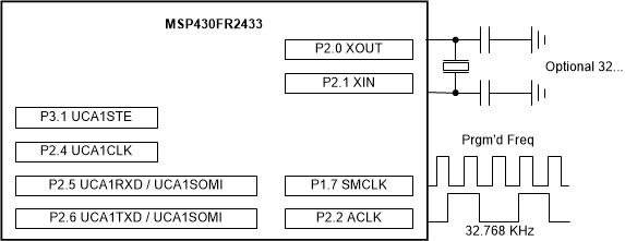
The clock system in the MSP430FR2433 device features an FLL that can be used to stabilize the internal DCO and achieve clock frequencies up to 16 MHz. The FLL requires a reference clock that can be sourced from either an internal 32.768-kHz reference oscillator (REFO) or an external crystal of the same frequency. However, TI recommends using a high-accuracy external 32.768-kHz crystal for best performance. Figure 1-1 shows the inputs and outputs of the programmable clock source.
 Figure 1-1 Programmable Clock Source
Inputs/Outputs
Figure 1-1 Programmable Clock Source
Inputs/OutputsAfter a device reset, the MSP430 MCU sources the subsystem master clock (SMCLK) from the DCO configured to run at 16 MHz. The device then executes a frequency command stored in FRAM that divides SMCLK to the last known frequency before device reset. This frequency is then output on P1.7, and the FLL reference is output on P2.2.
When the MSP430 MCU is first programmed, the default output frequency is 1 MHz. This default frequency can be altered by changing the initialization value of the command variable found in the accompanying software example. Then, as previously described, the MSP430 device will output the last known frequency upon device start-up. The programmable clock source can receive commands from a host processor through a 4800-baud UART or a 4-wire SPI. The UART interface uses P2.5 and P2.6 as receive and transmit respectively. The SPI uses P2.4, P2.5, P2.6 and P3.1. Table 1-1 lists the phase and polarity settings required for proper communication.
| Slave or Master | CLK Phase | CLK Polarity | CS Polarity |
|---|---|---|---|
| Slave | Data changed on first clock edge and captured on second | Inactive state is low | Active low |
Either interface allows a host processor to set the desired output frequency using any of the commands listed in Table 1-2. Each command is only one byte in length to maintain simplicity and reduce code size.
| Command Description | Hex Value |
|---|---|
| COMMAND_SET_1MHZ | 0x00 |
| COMMAND_SET_2MHZ | 0x02 |
| COMMAND_SET_4MHZ | 0x04 |
| COMMAND_SET_8MHZ | 0x06 |
| COMMAND_SET_16MHZ | 0x08 |
| COMMAND_GET_STATUS | 0x0A |
When using the UART interface, the MSP430 MCU will respond with a single byte when a command has completed execution. When using a SPI interface, the host processor must use COMMAND_GET_STATUS to query the execution status of the last command. Table 1-3 lists the three responses that can be issued from the programmable clock source.
| Response Description | Hex Value |
|---|---|
| Command executed successfully | 0x00 |
| Incorrect command | 0x01 |
| Command is still being processed | 0x02 |
A GUI can be used to configure the clock frequency. Figure 1-2 shows the block diagram for this implementation.
 Figure 1-2 Implementation
Overview
Figure 1-2 Implementation
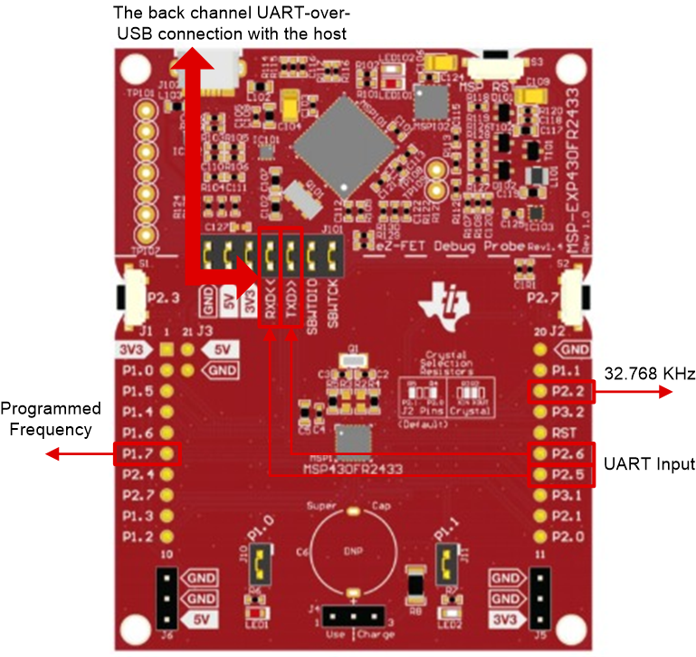
OverviewThe MSP430FR2433 LaunchPad Development Kit should be used with this example project. Backchannel UART interface on eZ-FET is used for UART communication with the GUI. To output clock at P1.7, use eUSCI_A1 peripheral instead of eUSCI_A0. A baud rate of 4800 must be selected with one stop bit and no parity. The COM channel number information can be found in the PC device management under the control panel. Figure 1-3 shows the MSP430FR2433 LaunchPad kit including eZ-FET, clock output and UART port.
 Figure 1-3 MSP430FR2433 LaunchPad
Development Kit
 The GUI is used to configure the frequency and displays the feedback information from MSP430. Figure 1-4 shows the overview of GUI. Below the scalar graph, there is a text box to display the feedback . On the bottom, there are 5 buttons which is used to choose the wanted clock source. When the button is clicked, the GUI will send a command to set the clock frequency and MSP430 will reply a data to show whether the frequency is set successfully.
 Figure 1-4 Programmable Clock Source
GUI
Figure 1-4 Programmable Clock Source
GUIPerformance
The programmable clock source can achieve 1-MHz, 2-MHz, 4-MHz, 8-MHz, or 16-MHz frequency output at ±2% accuracy using the internal REFO or ±0.5% accuracy using an external crystal. More detailed performance specifications can be found in the clock specifications section of the MSP430FR2433 MCU data sheet. Overall, the accuracy and power consumption is improved when using an external crystal oscillator.
In this application, the UART module receives its source clock from SMCLK. This was done so the baud rate registers need to be altered when the user changed the device frequency. Consequently, this increases the amount of code required to implement UART communication. However, because the MSP430 MCU acts as a slave, there are no such limitations when using SPI communication.
To Get Started
- Watch the training video “Programmable Clock Source With a Housekeeping MCU”, which shows how to use a GUI to adjust the clock frequency.
- Order a MSP430FR2433 LaunchPad kit to evaluate the programmable clock source example code.
- Download and test this example with the Programmable Clock Source example GUI.
- Evaluate the Programmable Clock Source example code for the MSP430FR2433 LaunchPad kit.
Device Recommendations
| Part Number | Key Features |
|---|---|
| MSP430FR2433 | 16KB FRAM, 4KB SRAM, 10-bit ADC, UART/SPI/I2C, Timer |
| MSP430FR2422 | 8KB FRAM, 2KB SRAM, 10-bit ADC, UART/SPI/I2C, Timer |
IMPORTANT NOTICE AND DISCLAIMER
| TI PROVIDES TECHNICAL AND RELIABILITY DATA (INCLUDING DATASHEETS), DESIGN RESOURCES (INCLUDING REFERENCE DESIGNS), APPLICATION OR OTHER DESIGN ADVICE, WEB TOOLS, SAFETY INFORMATION, AND OTHER RESOURCES “AS IS” AND WITH ALL FAULTS, AND DISCLAIMS ALL WARRANTIES, EXPRESS AND IMPLIED, INCLUDING WITHOUT LIMITATION ANY IMPLIED WARRANTIES OF MERCHANTABILITY, FITNESS FOR A PARTICULAR PURPOSE OR NON-INFRINGEMENT OF THIRD PARTY INTELLECTUAL PROPERTY RIGHTS. |
| These resources are intended for skilled developers designing with TI products. You are solely responsible for (1) selecting the appropriate TI products for your application, (2) designing, validating and testing your application, and (3) ensuring your application meets applicable standards, and any other safety, security, or other requirements. These resources are subject to change without notice. TI grants you permission to use these resources only for development of an application that uses the TI products described in the resource. Other reproduction and display of these resources is prohibited. No license is granted to any other TI intellectual property right or to any third party intellectual property right. TI disclaims responsibility for, and you will fully indemnify TI and its representatives against, any claims, damages, costs, losses, and liabilities arising out of your use of these resources. |
| TI’s products are provided subject to TI’s Terms of Sale (www.ti.com/legal/termsofsale.html) or other applicable terms available either on ti.com or provided in conjunction with such TI products. TI’s provision of these resources does not expand or otherwise alter TI’s applicable warranties or warranty disclaimers for TI products. |
| Mailing Address: Texas Instruments, Post Office Box 655303, Dallas, Texas 75265
Copyright © 2021, Texas Instruments Incorporated |