SLAAE46 November 2021 DAC43701
1 Introduction
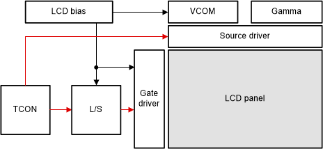
LCD panels are widely used in notebooks, TV, automotive display and so on. A typical LCD panel subsystem diagram block is shown in Figure 1-1. VCOM is the reference voltage for each pixel in the LCD panel. VCOM is typically used to maximize contrast and image quality during operation. A VCOM with different amplitudes and frequencies are needed to achieve different LCD electrical characteristics, optical characteristics and functional requirements.
 Figure 1-1 Typical LCD Panel Subsystem Diagram Block
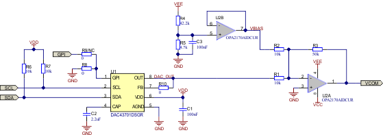
Figure 1-2 shows the LCD digital VCOM circuit using the DAC43701. It consists primarily of a DAC43701 and inverting summer circuit. The DAC output can be dynamically adjusted by I2C, and the inverting summer circuit outputs the required VCOM with specific gain and offset.
 Figure 1-2 LCD Digital VCOM Using the DAC43701
The DAC43701 uses the power supply (VDD) as a reference by default. It also contains an internal reference that can be enabled by writing a 1 to the REF_EN bit in the GENERAL_CONFIG register (address D1h). The DAC transfer function when VDD is used as reference is given in Equation 1.
Where, N is the DAC resolution, either 8-bits (DAC43701) or 10-bits (DAC53701). DAC_DATA is the decimal equivalent of the data in the DAC_DATA register (address 21h), ranges from 0 to 2N-1.
The transfer function of the inverting summer circuit is given in Equation 2.
Assuming R1 and R2 are equal, Equation 1 and Equation 2 became Equation 3
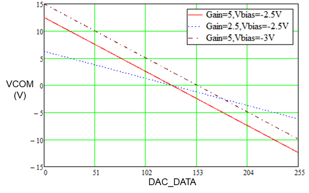
Thus, different amplitudes and frequencies of VCOM can be controlled by a dedicated DAC_DATA value, which is configured in real time by I2C. Figure 1-3 shows the VCOM voltage characteristic when VDD is 5 V.
 Figure 1-3 LCD Digital VCOM Voltage Characteristic