SLAAE76B march   2023  – june 2023 MSPM0G1105 , MSPM0G1106 , MSPM0G1107 , MSPM0G1505 , MSPM0G1506 , MSPM0G1507 , MSPM0G3105 , MSPM0G3106 , MSPM0G3107 , MSPM0G3505 , MSPM0G3506 , MSPM0G3507


  1.   1
  2.   Abstract
  3.   Trademarks
  4. MSPM0G Hardware Design Check List
  5. Power Supplies in MSPM0G Devices
    1. 2.1 Digital Power Supply
    2. 2.2 Analog Power Supply
    3. 2.3 Built-in Power Supply and Voltage Reference
    4. 2.4 Recommended Decoupling Circuit for Power Supply
  6. Reset and Power Supply Supervisor
    1. 3.1 Digital Power Supply
    2. 3.2 Power Supply Supervisor
  7. Clock System
    1. 4.1 Internal Oscillators
    2. 4.2 External Oscillators
    3. 4.3 External Clock Output (CLK_OUT)
    4. 4.4 Frequency Clock Counter (FCC)
  8. Debugger
    1. 5.1 Debug port pins and Pinout
    2. 5.2 Debug Port Connection With Standard JTAG Connector
  9. Key Analog Peripherals
    1. 6.1 ADC Design Considerations
    2. 6.2 OPA Design Considerations
    3. 6.3 DAC Design Considerations
    4. 6.4 COMP Design Considerations
    5. 6.5 GPAMP Design Considerations
  10. Key Digital Peripherals
    1. 7.1 Timer Resources and Design Considerations
    2. 7.2 UART and LIN Resources and Design Considerations
    3. 7.3 MCAN Design Considerations
    4. 7.4 I2C and SPI Design Considerations
  11. GPIOs
    1. 8.1 GPIO Output Switching Speed and Load Capacitance
    2. 8.2 GPIO Current Sink and Source
    3. 8.3 High-Speed GPIOs (HSIO)
    4. 8.4 High-Drive GPIOs (HDIO)
    5. 8.5 Open-Drain GPIOs Enable 5-V Communication Without a Level Shifter
    6. 8.6 Communicate With a 1.8-V Device Without a Level Shifter
    7. 8.7 Unused Pins Connection
  12. Layout Guides
    1. 9.1 Power Supply Layout
    2. 9.2 Considerations for Ground Layout
    3. 9.3 Traces, Vias, and Other PCB Components
    4. 9.4 How to Select Board Layers and Recommended Stack-up
  13. 10Bootloader
    1. 10.1 Bootloader Introduction
    2. 10.2 Bootloader Hardware Design Considerations
      1. 10.2.1 Physical Communication interfaces
      2. 10.2.2 Hardware Invocation
  14. 11References
  15. 12Revision History

Communicate With a 1.8-V Device Without a Level Shifter

The MSPM0G series devices use a 3.3-V logic level (excluding ODIO). If you need to communicate with 1.8-V devices and do not use external level shifter devices, Figure 8-2 shows a suggested circuit for interfacing with a 1.8-V device.
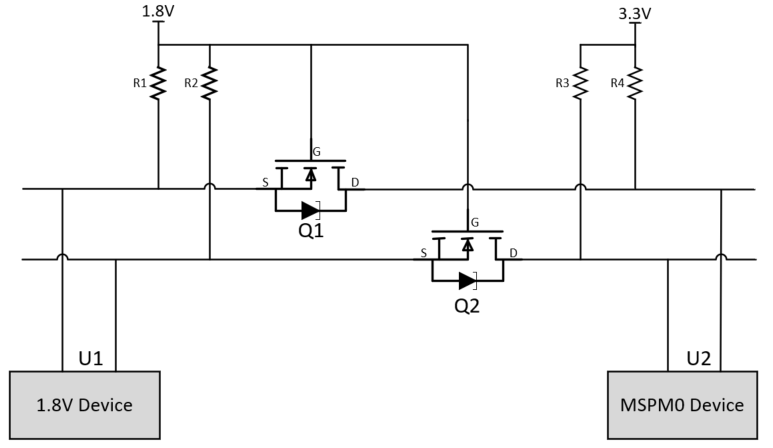
GUID-E55A0257-E08A-4231-88B1-49BC9B9B1ACF-low.png Figure 8-2 Suggested Communication Circuit With 1.8-V Device

Two MOSFET are used in this circuit - check the VGS to ensure this MOSFET can fully turn on with a low RDS(on): for 1.8-V device, use less than 1.8-V VGS MOSFET. However, too low VGS MOSFET, can cause the MOSFET to turn on at a very small voltage (MCU logic judges it as 0), resulting in communication logic error.

U1 output and U2 input

  1. U1 output “1.8v high”, Q1 VGS around 0, thus Q1 turn off, U2 reads “3.3v high” with R4.
  2. U1 output “low”, Q1 VGS around 1.8v, thus Q1 turn on, U2 reads “low”.

U1 input and U2 output

  1. U2 output “3.3 V high”, U1 keep 1.8 V with R1, and Q1 turn off, thus U1 reads “1.8 V high”.
  2. U2 output “low”, U1 keep 1.8 V with R1 firstly, but the diode inside MOSFET will pull down U1 to 0.7 V (diode voltage drops), and then cause VGS to be greater than the turn-on voltage, Q1 turns on, and U1 reads "low".