SLAAE76B march   2023  – june 2023 MSPM0G1105 , MSPM0G1106 , MSPM0G1107 , MSPM0G1505 , MSPM0G1506 , MSPM0G1507 , MSPM0G3105 , MSPM0G3106 , MSPM0G3107 , MSPM0G3505 , MSPM0G3506 , MSPM0G3507


  1.   1
  2.   Abstract
  3.   Trademarks
  4. MSPM0G Hardware Design Check List
  5. Power Supplies in MSPM0G Devices
    1. 2.1 Digital Power Supply
    2. 2.2 Analog Power Supply
    3. 2.3 Built-in Power Supply and Voltage Reference
    4. 2.4 Recommended Decoupling Circuit for Power Supply
  6. Reset and Power Supply Supervisor
    1. 3.1 Digital Power Supply
    2. 3.2 Power Supply Supervisor
  7. Clock System
    1. 4.1 Internal Oscillators
    2. 4.2 External Oscillators
    3. 4.3 External Clock Output (CLK_OUT)
    4. 4.4 Frequency Clock Counter (FCC)
  8. Debugger
    1. 5.1 Debug port pins and Pinout
    2. 5.2 Debug Port Connection With Standard JTAG Connector
  9. Key Analog Peripherals
    1. 6.1 ADC Design Considerations
    2. 6.2 OPA Design Considerations
    3. 6.3 DAC Design Considerations
    4. 6.4 COMP Design Considerations
    5. 6.5 GPAMP Design Considerations
  10. Key Digital Peripherals
    1. 7.1 Timer Resources and Design Considerations
    2. 7.2 UART and LIN Resources and Design Considerations
    3. 7.3 MCAN Design Considerations
    4. 7.4 I2C and SPI Design Considerations
  11. GPIOs
    1. 8.1 GPIO Output Switching Speed and Load Capacitance
    2. 8.2 GPIO Current Sink and Source
    3. 8.3 High-Speed GPIOs (HSIO)
    4. 8.4 High-Drive GPIOs (HDIO)
    5. 8.5 Open-Drain GPIOs Enable 5-V Communication Without a Level Shifter
    6. 8.6 Communicate With a 1.8-V Device Without a Level Shifter
    7. 8.7 Unused Pins Connection
  12. Layout Guides
    1. 9.1 Power Supply Layout
    2. 9.2 Considerations for Ground Layout
    3. 9.3 Traces, Vias, and Other PCB Components
    4. 9.4 How to Select Board Layers and Recommended Stack-up
  13. 10Bootloader
    1. 10.1 Bootloader Introduction
    2. 10.2 Bootloader Hardware Design Considerations
      1. 10.2.1 Physical Communication interfaces
      2. 10.2.2 Hardware Invocation
  14. 11References
  15. 12Revision History

Power Supply Layout

Figure 9-1 shows the typical parts placement and routing for the power supply layout; you must modify this appropriately for your MSPM0G part. You can optionally connect a filter inductor in series with the VCC and MCU VDD pins. This inductor is used to filter the switching noise frequency of DCDC. For the value, please refer to the data sheet of DCDC vendor. C1/C2/C3 values and layout in the MSPM0G device data sheets.

Note:
  • Keep the smallest capacitance, closest to the MCU VDD pin (C1 < C2 < C3).
  • Make all the traces direct without any vias.
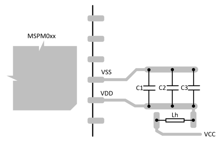
GUID-A6FC6253-9018-461B-9534-64BA02878D53-low.png Figure 9-1 Suggested Power Supply Layout