SLAAE76B march 2023 – june 2023 MSPM0G1105 , MSPM0G1106 , MSPM0G1107 , MSPM0G1505 , MSPM0G1506 , MSPM0G1507 , MSPM0G3105 , MSPM0G3106 , MSPM0G3107 , MSPM0G3505 , MSPM0G3506 , MSPM0G3507
4.2 External Oscillators
For applications that require even higher clock accuracy across devices and temperature, external oscillators can be used. LFXT can replace LFOSC, and HFXT can replace SYSOSC.
Low-Frequency Crystal Oscillator (LFXT)
The LFXT is an ultra-low power crystal oscillator that supports driving a standard 32.768-kHz watch crystal. To use the LFXT, populate a watch crystal between the LFXIN and LFXOUT pins. Place loading capacitors on both LFXIN and LFXOUT pins to circuit ground (VSS). Size the crystal load capacitors according to the specifications of the crystal being used. A variety of crystal types are supported through a programmable drive strength mechanism. For the layout advice, see Section 9.
 Figure 4-4 MSPM0G LFXT Circuit
LFCLK_IN (Digital Clock)
The LFXT circuit can be bypassed and a 32.76-kHz typical frequency digital clock can be brought into the device to use as the LFCLK source. LFCLK_IN and LFXT are mutually exclusive and must not be enabled at the same time.
LFCLK_IN is compatible with digital square-wave CMOS clock inputs with a typical duty cycle of 50%. It is possible to check for a valid clock signal on LFCLK_IN by enabling the LFCLK monitor. By default, the LFCLK monitor checks LFCLK_IN if the LFXT was not started.
High-Frequency Crystal Oscillator (HFXT)
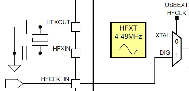
The high frequency crystal oscillator (HFXT) can be used with standard crystals and resonators in the 4- to 48-MHz range to generate a stable high-speed reference clock for the system.
To use the HFXT, populate a crystal or resonator between the HFXIN and HFXOUT pins. Place loading capacitors on both pins to circuit ground (VSS). Size the crystal load capacitors according to the specifications of the crystal being used. A programmable HFXT startup time is provided with 64-µs resolution. For layout advice, see Section 9.
 Figure 4-5 MSPM0G HFXT Circuit
HFCLK_IN (Digital clock)
It is possible to bypass the HFXT circuit and bring in a 4- to 48-MHz typical frequency digital clock into the device to use as the HFCLK source instead of HFXT. HFCLK_IN and HFXT are mutually exclusive and must not be enabled at the same time.
HFCLK_IN is compatible with digital square wave CMOS clock inputs with a typical duty cycle of 50%.