SLAAE76B march   2023  – june 2023 MSPM0G1105 , MSPM0G1106 , MSPM0G1107 , MSPM0G1505 , MSPM0G1506 , MSPM0G1507 , MSPM0G3105 , MSPM0G3106 , MSPM0G3107 , MSPM0G3505 , MSPM0G3506 , MSPM0G3507


  1.   1
  2.   Abstract
  3.   Trademarks
  4. MSPM0G Hardware Design Check List
  5. Power Supplies in MSPM0G Devices
    1. 2.1 Digital Power Supply
    2. 2.2 Analog Power Supply
    3. 2.3 Built-in Power Supply and Voltage Reference
    4. 2.4 Recommended Decoupling Circuit for Power Supply
  6. Reset and Power Supply Supervisor
    1. 3.1 Digital Power Supply
    2. 3.2 Power Supply Supervisor
  7. Clock System
    1. 4.1 Internal Oscillators
    2. 4.2 External Oscillators
    3. 4.3 External Clock Output (CLK_OUT)
    4. 4.4 Frequency Clock Counter (FCC)
  8. Debugger
    1. 5.1 Debug port pins and Pinout
    2. 5.2 Debug Port Connection With Standard JTAG Connector
  9. Key Analog Peripherals
    1. 6.1 ADC Design Considerations
    2. 6.2 OPA Design Considerations
    3. 6.3 DAC Design Considerations
    4. 6.4 COMP Design Considerations
    5. 6.5 GPAMP Design Considerations
  10. Key Digital Peripherals
    1. 7.1 Timer Resources and Design Considerations
    2. 7.2 UART and LIN Resources and Design Considerations
    3. 7.3 MCAN Design Considerations
    4. 7.4 I2C and SPI Design Considerations
  11. GPIOs
    1. 8.1 GPIO Output Switching Speed and Load Capacitance
    2. 8.2 GPIO Current Sink and Source
    3. 8.3 High-Speed GPIOs (HSIO)
    4. 8.4 High-Drive GPIOs (HDIO)
    5. 8.5 Open-Drain GPIOs Enable 5-V Communication Without a Level Shifter
    6. 8.6 Communicate With a 1.8-V Device Without a Level Shifter
    7. 8.7 Unused Pins Connection
  12. Layout Guides
    1. 9.1 Power Supply Layout
    2. 9.2 Considerations for Ground Layout
    3. 9.3 Traces, Vias, and Other PCB Components
    4. 9.4 How to Select Board Layers and Recommended Stack-up
  13. 10Bootloader
    1. 10.1 Bootloader Introduction
    2. 10.2 Bootloader Hardware Design Considerations
      1. 10.2.1 Physical Communication interfaces
      2. 10.2.2 Hardware Invocation
  14. 11References
  15. 12Revision History

DAC Design Considerations

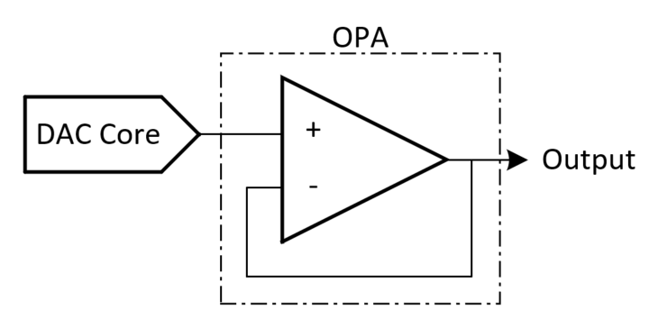
MSPM0G devices include two DAC modules: 8-bit and 12-bit. The DAC can be used as the reference voltage and also can work with the OPA to drive the output pad directly. 12-bit DAC modules include a buffer, thus this can output to pad directly. However, the 8-bit DAC module is normally used as internal reference voltage for OPA and COMP, therefore to output to an external pin, the OPA must be configured into buffer mode to improve the drive strength.

Not all devices include these two DAC modules. See the device-specific data sheet for details.

GUID-20221017-SS0I-DSQX-LSKP-GHSZNZPZPCV3-low.svg Figure 6-4 8-Bit DAC Block Diagram
GUID-A843BC18-B8FE-467F-893F-D5C1BD8822BA-low.png Figure 6-5 8-Bit DAC and OPA Output Block Diagram
GUID-05602A46-CA06-4649-8316-CF214C0A835B-low.png Figure 6-6 12-bit DAC Output Block Diagram