SLAAE76B march   2023  – june 2023 MSPM0G1105 , MSPM0G1106 , MSPM0G1107 , MSPM0G1505 , MSPM0G1506 , MSPM0G1507 , MSPM0G3105 , MSPM0G3106 , MSPM0G3107 , MSPM0G3505 , MSPM0G3506 , MSPM0G3507


  1.   1
  2.   Abstract
  3.   Trademarks
  4. MSPM0G Hardware Design Check List
  5. Power Supplies in MSPM0G Devices
    1. 2.1 Digital Power Supply
    2. 2.2 Analog Power Supply
    3. 2.3 Built-in Power Supply and Voltage Reference
    4. 2.4 Recommended Decoupling Circuit for Power Supply
  6. Reset and Power Supply Supervisor
    1. 3.1 Digital Power Supply
    2. 3.2 Power Supply Supervisor
  7. Clock System
    1. 4.1 Internal Oscillators
    2. 4.2 External Oscillators
    3. 4.3 External Clock Output (CLK_OUT)
    4. 4.4 Frequency Clock Counter (FCC)
  8. Debugger
    1. 5.1 Debug port pins and Pinout
    2. 5.2 Debug Port Connection With Standard JTAG Connector
  9. Key Analog Peripherals
    1. 6.1 ADC Design Considerations
    2. 6.2 OPA Design Considerations
    3. 6.3 DAC Design Considerations
    4. 6.4 COMP Design Considerations
    5. 6.5 GPAMP Design Considerations
  10. Key Digital Peripherals
    1. 7.1 Timer Resources and Design Considerations
    2. 7.2 UART and LIN Resources and Design Considerations
    3. 7.3 MCAN Design Considerations
    4. 7.4 I2C and SPI Design Considerations
  11. GPIOs
    1. 8.1 GPIO Output Switching Speed and Load Capacitance
    2. 8.2 GPIO Current Sink and Source
    3. 8.3 High-Speed GPIOs (HSIO)
    4. 8.4 High-Drive GPIOs (HDIO)
    5. 8.5 Open-Drain GPIOs Enable 5-V Communication Without a Level Shifter
    6. 8.6 Communicate With a 1.8-V Device Without a Level Shifter
    7. 8.7 Unused Pins Connection
  12. Layout Guides
    1. 9.1 Power Supply Layout
    2. 9.2 Considerations for Ground Layout
    3. 9.3 Traces, Vias, and Other PCB Components
    4. 9.4 How to Select Board Layers and Recommended Stack-up
  13. 10Bootloader
    1. 10.1 Bootloader Introduction
    2. 10.2 Bootloader Hardware Design Considerations
      1. 10.2.1 Physical Communication interfaces
      2. 10.2.2 Hardware Invocation
  14. 11References
  15. 12Revision History

Built-in Power Supply and Voltage Reference

The VREF module for the MSPM0G family is a shared voltage reference module that can be leveraged by a variety on on-board analog peripherals.

The VREF module features include:

  • 1.4-V and 2.5-V user-selectable internal references.
  • Support for receiving external reference on the VREF+ and VREF- device pins.
  • Sample and hold mode support VREF operation down to STANDBY operating mode.
  • Internal reference supports for ADC, COMP, and OPA.

When supplying the MCU with an external reference, TI recommends connecting a decoupling capacitor on the reference pins with a value based on the voltage source (see Figure 2-2).
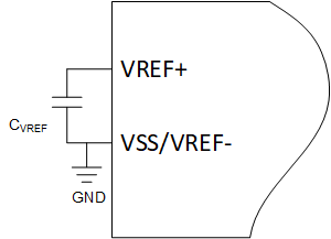
GUID-9D3216A1-6E2E-45EB-B84B-10E60FB2EBC3-low.png Figure 2-2 VREF Circuit