SLAAE76B march   2023  – june 2023 MSPM0G1105 , MSPM0G1106 , MSPM0G1107 , MSPM0G1505 , MSPM0G1506 , MSPM0G1507 , MSPM0G3105 , MSPM0G3106 , MSPM0G3107 , MSPM0G3505 , MSPM0G3506 , MSPM0G3507


  1.   1
  2.   Abstract
  3.   Trademarks
  4. MSPM0G Hardware Design Check List
  5. Power Supplies in MSPM0G Devices
    1. 2.1 Digital Power Supply
    2. 2.2 Analog Power Supply
    3. 2.3 Built-in Power Supply and Voltage Reference
    4. 2.4 Recommended Decoupling Circuit for Power Supply
  6. Reset and Power Supply Supervisor
    1. 3.1 Digital Power Supply
    2. 3.2 Power Supply Supervisor
  7. Clock System
    1. 4.1 Internal Oscillators
    2. 4.2 External Oscillators
    3. 4.3 External Clock Output (CLK_OUT)
    4. 4.4 Frequency Clock Counter (FCC)
  8. Debugger
    1. 5.1 Debug port pins and Pinout
    2. 5.2 Debug Port Connection With Standard JTAG Connector
  9. Key Analog Peripherals
    1. 6.1 ADC Design Considerations
    2. 6.2 OPA Design Considerations
    3. 6.3 DAC Design Considerations
    4. 6.4 COMP Design Considerations
    5. 6.5 GPAMP Design Considerations
  10. Key Digital Peripherals
    1. 7.1 Timer Resources and Design Considerations
    2. 7.2 UART and LIN Resources and Design Considerations
    3. 7.3 MCAN Design Considerations
    4. 7.4 I2C and SPI Design Considerations
  11. GPIOs
    1. 8.1 GPIO Output Switching Speed and Load Capacitance
    2. 8.2 GPIO Current Sink and Source
    3. 8.3 High-Speed GPIOs (HSIO)
    4. 8.4 High-Drive GPIOs (HDIO)
    5. 8.5 Open-Drain GPIOs Enable 5-V Communication Without a Level Shifter
    6. 8.6 Communicate With a 1.8-V Device Without a Level Shifter
    7. 8.7 Unused Pins Connection
  12. Layout Guides
    1. 9.1 Power Supply Layout
    2. 9.2 Considerations for Ground Layout
    3. 9.3 Traces, Vias, and Other PCB Components
    4. 9.4 How to Select Board Layers and Recommended Stack-up
  13. 10Bootloader
    1. 10.1 Bootloader Introduction
    2. 10.2 Bootloader Hardware Design Considerations
      1. 10.2.1 Physical Communication interfaces
      2. 10.2.2 Hardware Invocation
  14. 11References
  15. 12Revision History

Digital Power Supply

VCORE Regulator

An internal low-dropout linear voltage regulator generates a 1.35-V supply rail to power the device core. In general, the core regulator output (VCORE) supplies power to the core logic, which includes the CPU, digital peripherals and the device memory. The core regulator requires an external capacitor (CVCORE) which is connected between the device VCORE pin and VSS (ground) (see Figure 2-1). See the device-specific data sheet for the correct value and tolerance of CVCORE. CVCORE should be placed close to the VCORE pin.

The core regulator is active in all power modes except for SHUTDOWN. In all other power modes (RUN, SLEEP, STOP, and STANDBY) the drive strength of the regulator is configured automatically to support the max load current of each mode. This reduces the quiescent current of the regulator when using low power modes, improving low power performance.
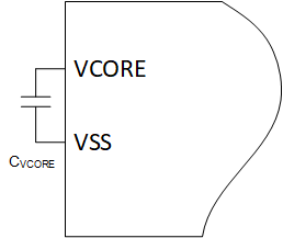
GUID-0FB791A9-8601-4F24-920D-D36409F2A23B-low.png Figure 2-1 VCORE Regulator Circuit