SLAAED4 October 2023 TAA5412-Q1 , TAC5311-Q1 , TAC5312-Q1 , TAC5411-Q1 , TAC5412-Q1
2.3 Differential DC Coupled Configuration
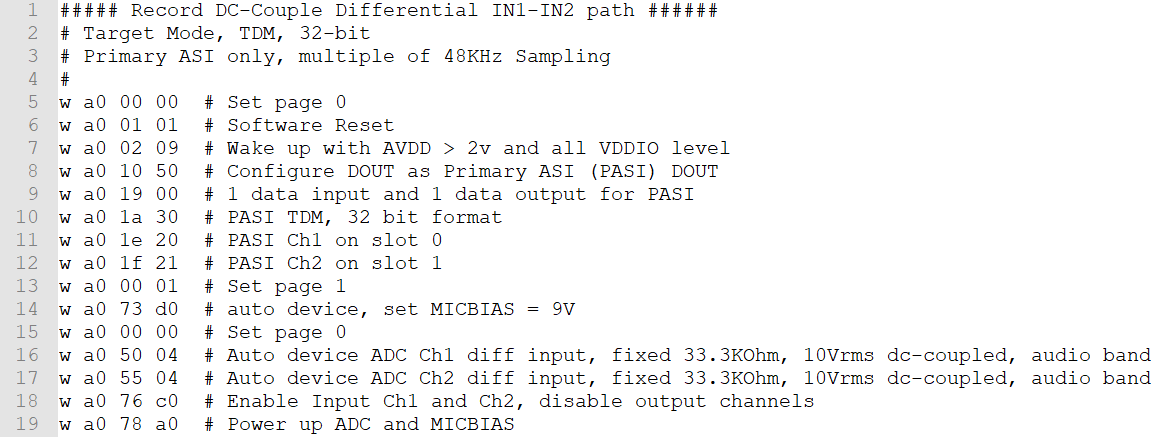
In the DC-Coupled differential input configuration, the following device register setting is used and the input waveform provided to IN1P/M for the full-scale swing with 6 V Vcm.
 Figure 2-10 Differential DC-Coupled
Register Setting
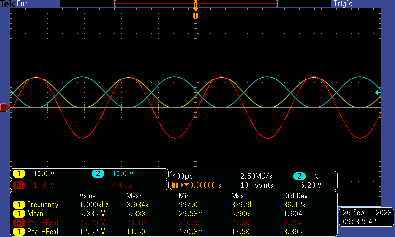
 Figure 2-11 Differential DC-Coupled
Input Swing at -1dBrG (0dBrG = 10Vrms)
Figure 2-11 Differential DC-Coupled
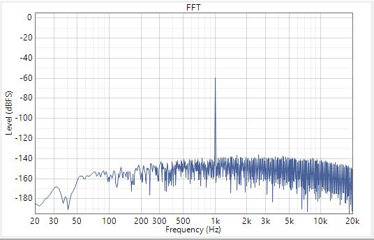
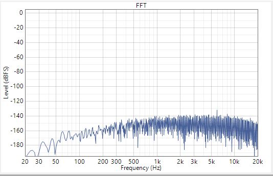
Input Swing at -1dBrG (0dBrG = 10Vrms)A frequency plot of the Dynamic Range with -60dBrG input and SNR with input AC signal shorted to ground are provided here of the 1Vpp common-mode setting. A similar plot can be obtained for supply common-mode tolerances.
 Figure 2-12 Differential DC-Coupled
Dynamic Range at -60dBrG Input
 Figure 2-13 SNR with Input AC Signal
shorted to GND
Figure 2-13 SNR with Input AC Signal
shorted to GNDTable 2-3 summarizes the performances for the different device variants.
Table 2-3 Device Variants
| THDN (at-1dBrG) | DR (dB) | SNR (dB) | ||||||
|---|---|---|---|---|---|---|---|---|
| TAC541x | TAA541x | TAC531x | TAC541x | TAA541x | TAC531x | TAC541x | TAA541x | TAC531x |
| -101 | -100 | -89 | 112 | 112 | 101 | 112 | 112 | 101 |