SLAAED4 October 2023 TAA5412-Q1 , TAC5311-Q1 , TAC5312-Q1 , TAC5411-Q1 , TAC5412-Q1
2.5 Analog Input Mux Configuration
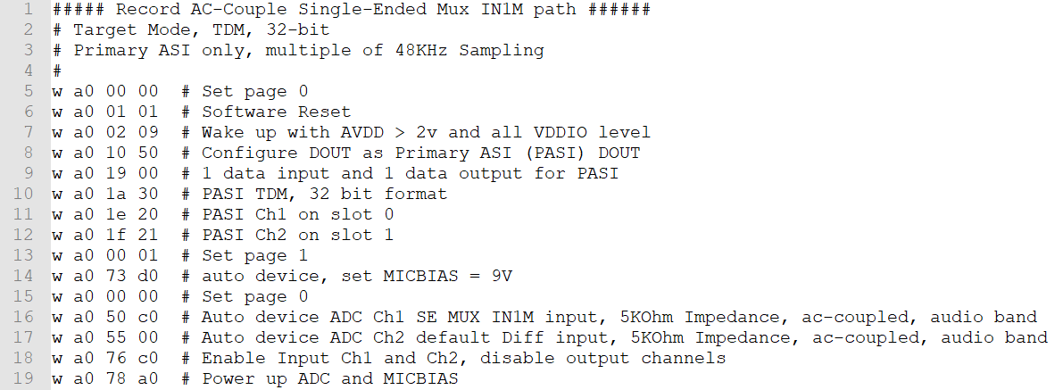
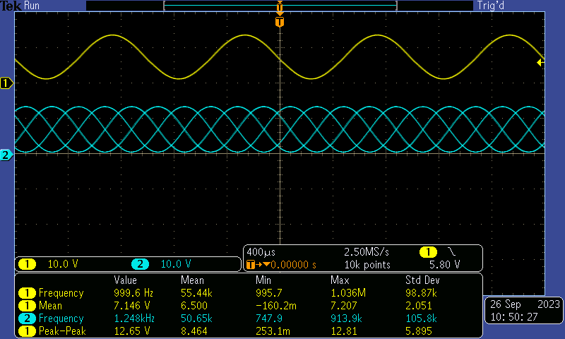
Analog mux input allows input selection either from IN1P or IN1M into the ADC path. The device needs to be configured in the respective mux setting in register B0_P0_R80 (0x50) ADC_CH1_INSRC. In this configuration, either IN1P or IN1M be the input to the ADC signal chain, they are independent source. In this example, IN1P is a 1 KHz tone at -1 dBrG and IN1M is a 1250 Hz tone at -1 dBrG; 0 dBrG = 5 Vrms Single-Ended Full-scale.
 Figure 2-18 IN1P Mux Input Register Setting
 Figure 2-19 IN1M Mux Input Register Setting
 Figure 2-20 IN1P and IN1M Mux Input at -1dBrG (0 dBrG =
5Vrms)
Figure 2-20 IN1P and IN1M Mux Input at -1dBrG (0 dBrG =
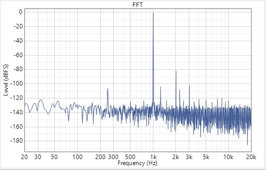
5Vrms)The output of the respective setting shows the desired signal and the suppression of the other input signal.
 Figure 2-21 Output with IN1P Mux Input Configured
 Figure 2-22 Output with IN1M Mux Input Configured