SLAAEE6 October 2023 MSPM0L1306 , MSPM0L1306
5 Current Detection and Calibration Method
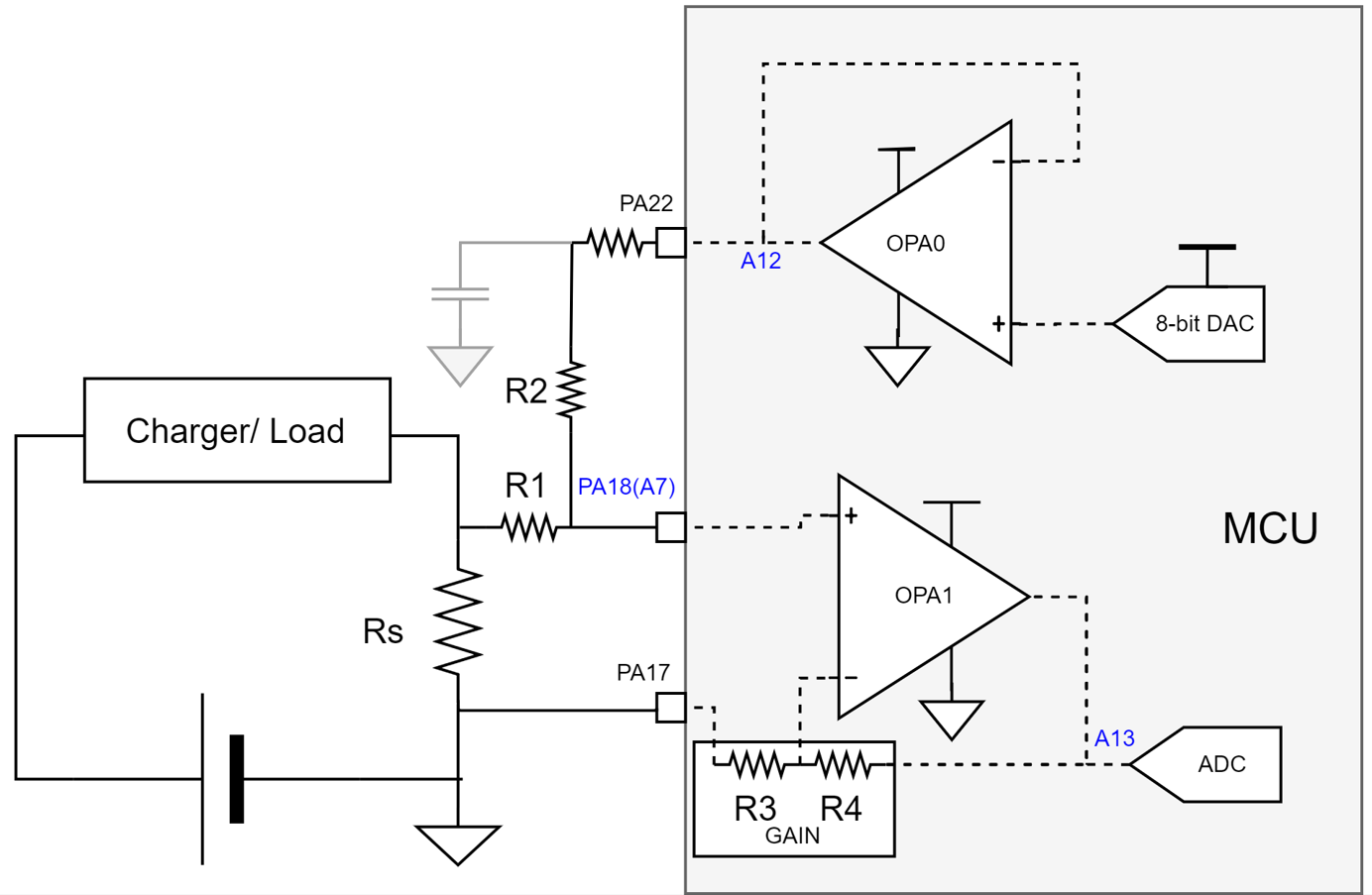
Here is the current detection block diagram. We can see that this solution utilizes:
- Two high precision internal OPAs. One OPA used as a buffer for DAC. Another used to generate gain for the voltage across the shunter resistor.
- One internal DAC. Used to generate dynamic bias voltage for current detection paired with OPA0.
- Flexible internal gain, which is the key point to realize different detection range. If you increase the gain, then the detection range will be smaller, but its resolution will be increased as well.
- Internal SAR ADC. Used to calibrate and detect the voltage output from OPA0.
 Figure 5-1 Current Detection Block
Diagram