SLAAEE6 October   2023 MSPM0L1306 , MSPM0L1306


  1.   1
  2.   Abstract
  3.   Trademarks
  4. 1Introduction
  5. 2Hardware Introduction
  6. 3Software Introduction
  7. 4Gauge GUI Introduction
  8. 5Current Detection and Calibration Method
    1. 5.1 MSPM0 OPA Introduction
      1. 5.1.1 OPA input and output limitation
      2. 5.1.2 OPA Accuracy Influence
    2. 5.2 Current Detection Method
    3. 5.3 Current Calibration Method
      1. 5.3.1 (R1+R2)/R2 calibration
      2. 5.3.2 OPA1 Voffset calibration
      3. 5.3.3 R3/(R4+R3) calibration
      4. 5.3.4 Vref calibration
  9. 6Solution Evaluation Steps
    1. 6.1 Step1: Hardware Preparation
    2. 6.2 Step2: Evaluation
  10. 7MSPM0 Gauge Solution Test Results
    1. 7.1 Calibration Test Result
    2. 7.2 Current Detection Result
      1. 7.2.1 Test Under 25°C
      2. 7.2.2 Test Under 0°C
      3. 7.2.3 Test Under 50°C
      4. 7.2.4 Conclusion
    3. 7.3 Current Consumption Test
  11. 8Solution Summery and Improvement Direction
    1. 8.1 Shunter Resistor
    2. 8.2 ADC and its Reference
    3. 8.3 Runtime Calibration

Hardware Introduction

Figure 2-1 is a hardware high-level block diagram, showing all the used pins by this demo. The solution demonstrates testing the current at ADC channel 13, the temperature at ADC channel5 and voltage at ADC channel1.
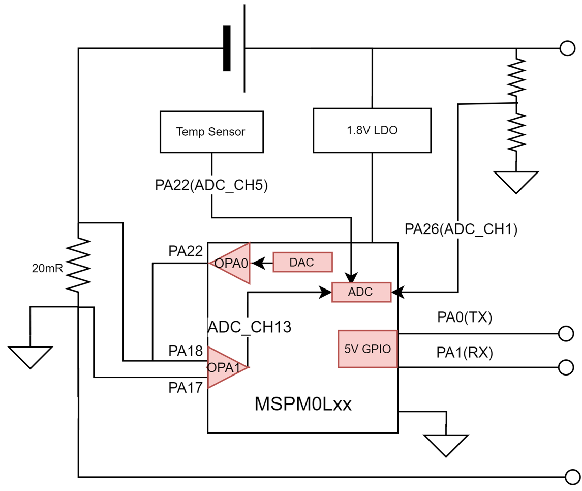
GUID-8E826C40-ED53-40A4-BDCD-3FCC931B58F2-low.png Figure 2-1 MSPM0 Gauge Board Block Diagram

This design can use these MSPM0 features:

  • High precision 12-bit ADC for temperature, current and voltage detection.
  • Integrated high precision chopper OPAs for current detection.
  • 5 V tolerant open-drain I/O with UART or I2C function to communicate with masters under different power rails.
  • Lower to 1.62 V working voltage to support single battery full voltage range.
  • Lower to 1.1 µA STANDBY current with SRAM retention for battery application,

Here, a quick introduction for the hardware board is provided and how to use it. For the battery, you can insert it into the default socket or connect it to the backup battery supply input. Debug and UART COM port is used to connect to PC, which can download the code or communicate with the GUI.
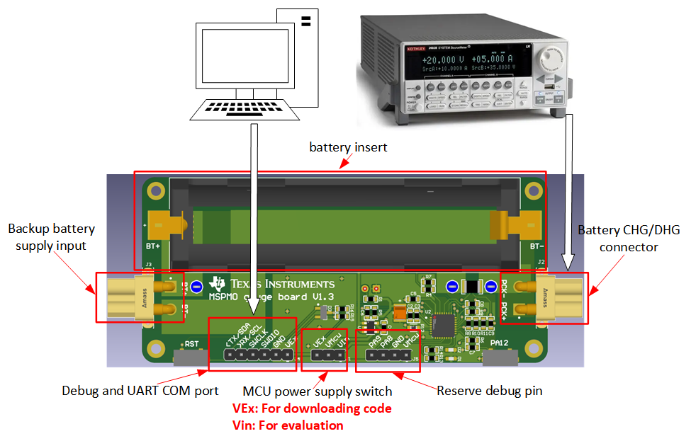
Note: Pay attention to the MCU power switch supply jumper. For downloading, connect VMCU to VEx, then the MCU are supplied with 3.3 V, which can ensure the voltage matching with the debugger. For evaluation, connect VMCU to VIn, then the MCU is supplied with 1.8 V LDO. It can ensure the best analog performance.
GUID-67653F3F-5DC1-4DCA-82B6-B91B1A4B2773-low.png Figure 2-2 Gauge Board Instructions