SLAAEG4 October   2023 MSPM0C1104 , MSPM0L1306


  1.   1
  2.   Abstract
  3.   Trademarks
  4. MSPM0C Hardware Design Check List
  5. Power Supplies in MSPM0C Devices
    1. 2.1 Digital Power Supply
    2. 2.2 Analog Power Supply
    3. 2.3 Built-in Power Supply and Voltage Reference
    4. 2.4 Recommended Decoupling Circuit for Power Supply
  6. Reset and Power Supply Supervisor
    1. 3.1 Digital Power Supply
    2. 3.2 Power Supply Supervisor
      1. 3.2.1 Power-On Reset (POR) Monitor
      2. 3.2.2 Brownout Reset (BOR) Monitor
      3. 3.2.3 POR and BOR Behavior During Supply Changes
  7. Clock System
    1. 4.1 Internal Oscillators
      1. 4.1.1 Internal Low-Frequency Oscillator (LFOSC)
      2. 4.1.2 Internal System Oscillator (SYSOSC)
    2. 4.2 External Clock Input (xFCLK_IN)
      1. 4.2.1 LFCLK_IN
      2. 4.2.2 HFCLK_IN
    3. 4.3 External Clock Output (CLK_OUT)
    4. 4.4 Frequency Clock Counter (FCC)
  8. Debugger
    1. 5.1 Debug Port Pins and Pinout
    2. 5.2 Debug Port Connection With Standard JTAG Connector
      1. 5.2.1 Standard XDS110
      2. 5.2.2 Lite XDS110 (MSPM0 LaunchPad™ kit)
  9. Key Analog Peripherals
    1. 6.1 ADC Design Considerations
  10. Key Digital Peripherals
    1. 7.1 Timer Resources and Design Considerations
    2. 7.2 UART and LIN Resources and Design Considerations
    3. 7.3 I2C and SPI Design Considerations
  11. GPIOs
    1. 8.1 GPIO Output Switching Speed and Load Capacitance
    2. 8.2 GPIO Current Sink and Source
    3. 8.3 Open-Drain GPIOs Enable 5-V Communication Without a Level Shifter
    4. 8.4 Communicate With 1.8-V Devices Without a Level Shifter
    5. 8.5 Unused Pins Connection
  12. Layout Guides
    1. 9.1 Power Supply Layout
    2. 9.2 Considerations for Ground Layout
      1. 9.2.1 What is Ground Noise?
    3. 9.3 Traces, Vias, and Other PCB Components
    4. 9.4 How to Select Board Layers and Recommended Stack-up
  13. 10References

MSPM0C Hardware Design Check List

Table 1-1 describes the main signal that needs to be checked during the MSPM0C hardware design process. The following sections provide more details.

Table 1-1 MSPM0C Hardware Design Check List
Pin (1) Description Requirements
VDD Power supply positive pin Place 10-µF and 100-nF capacitors between VDD and VSS, and keep those part close to VDD and VSS.
VSS Power supply negative pin
NRST Reset pin Connect an external 47-kΩ pullup resistor with a 10-nF pulldown capacitor.
SWCLK Serial wire clock from debug probe Internal pulldown to VDD, does not need any external part.
SWDIO Bidirectional (shared) serial wire data Internal pullup to VSS, does not need any external part.
PA0, PA1 Open-drain I/O Pull-up resistor required for output high
PAx (exclude PA0, PA1) General-purpose I/O Set corresponding pin functions to GPIO (PINCMx.PF = 0x1) and configure unused pins to output low or input with internal pullup or pulldown resistor.
For any unused pin with a function that is shared with general-purpose I/O, follow the Section 8.5.

TI recommends connecting a combination of a 10-μF and a 0.1-nF low-ESR ceramic decoupling capacitor to the VDD and VSS pins. Higher-value capacitors can be used but can impact supply rail ramp-up time. Decoupling capacitors must be placed as close as possible to the decoupled pins (within a few millimeters).

The NRST reset pin is required to connect an external 47-kΩ pullup resistor with a 10-nF pulldown capacitor.

For 5-V-tolerant open drain (ODIO), a pullup resistor is required to output high, this is required for inter-integrated circuit (I2C) and universal asynchronous receiver/transmitter (UART) functions if the ODIO are used.
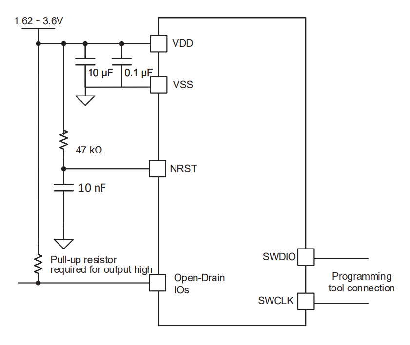
GUID-A9D60E5A-BC0D-4D12-90A4-C4F9843EC489-low.png Figure 1-1 MSPM0C Typical Application Schematic