SLAAEG4 October   2023 MSPM0C1104 , MSPM0L1306


  1.   1
  2.   Abstract
  3.   Trademarks
  4. MSPM0C Hardware Design Check List
  5. Power Supplies in MSPM0C Devices
    1. 2.1 Digital Power Supply
    2. 2.2 Analog Power Supply
    3. 2.3 Built-in Power Supply and Voltage Reference
    4. 2.4 Recommended Decoupling Circuit for Power Supply
  6. Reset and Power Supply Supervisor
    1. 3.1 Digital Power Supply
    2. 3.2 Power Supply Supervisor
      1. 3.2.1 Power-On Reset (POR) Monitor
      2. 3.2.2 Brownout Reset (BOR) Monitor
      3. 3.2.3 POR and BOR Behavior During Supply Changes
  7. Clock System
    1. 4.1 Internal Oscillators
      1. 4.1.1 Internal Low-Frequency Oscillator (LFOSC)
      2. 4.1.2 Internal System Oscillator (SYSOSC)
    2. 4.2 External Clock Input (xFCLK_IN)
      1. 4.2.1 LFCLK_IN
      2. 4.2.2 HFCLK_IN
    3. 4.3 External Clock Output (CLK_OUT)
    4. 4.4 Frequency Clock Counter (FCC)
  8. Debugger
    1. 5.1 Debug Port Pins and Pinout
    2. 5.2 Debug Port Connection With Standard JTAG Connector
      1. 5.2.1 Standard XDS110
      2. 5.2.2 Lite XDS110 (MSPM0 LaunchPad™ kit)
  9. Key Analog Peripherals
    1. 6.1 ADC Design Considerations
  10. Key Digital Peripherals
    1. 7.1 Timer Resources and Design Considerations
    2. 7.2 UART and LIN Resources and Design Considerations
    3. 7.3 I2C and SPI Design Considerations
  11. GPIOs
    1. 8.1 GPIO Output Switching Speed and Load Capacitance
    2. 8.2 GPIO Current Sink and Source
    3. 8.3 Open-Drain GPIOs Enable 5-V Communication Without a Level Shifter
    4. 8.4 Communicate With 1.8-V Devices Without a Level Shifter
    5. 8.5 Unused Pins Connection
  12. Layout Guides
    1. 9.1 Power Supply Layout
    2. 9.2 Considerations for Ground Layout
      1. 9.2.1 What is Ground Noise?
    3. 9.3 Traces, Vias, and Other PCB Components
    4. 9.4 How to Select Board Layers and Recommended Stack-up
  13. 10References

Communicate With 1.8-V Devices Without a Level Shifter

The MSPM0C series devices use a 3.3-V logic level (excluding ODIO). To communicate with 1.8-V devices without an external level shifter device, Figure 8-2 shows a suggested circuit for interfacing with a 1.8-V device.
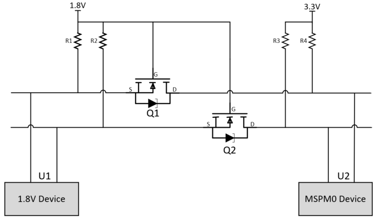
GUID-FFAE15CD-6B15-4DB4-BD33-C32AFE848926-low.png Figure 8-2 Suggested Communication Circuit With 1.8-V Device

Two MOSFET are used in this circuit - check the VGS to ensure this MOSFET be able to fully turn on with a low RDS(on): for a 1.8-V device, use less than 1.8-V VGS MOSFET. However, do not use a too low VGS MOSFET, as this causes the MOSFET to turn on at a very small voltage (MCU logic judges it as 0), resulting in communication logic error.

U1 output and U2 input

  1. U1 output "1.8 V high", Q1 VGS around 0, thus Q1 turn off, U2 reads "3.3 V high" with R4.
  2. U1 output "low", Q1 VGS near 1.8 V, thus Q1 turn on, U2 reads "low".

U1 input and U2 output

  1. U2 output "3.3 V high", U1 keeps 1.8 V with R1, and Q1 turns off, thus U1 reads "1.8 V high".
  2. U2 output "low", U1 keeps 1.8 V with R1 at first, but the diode in the MOSFET pulls down U1 to 0.7 V (diode voltage drops), and then causes VGS to be greater than the turn-on voltage, Q1 turns on, and U1 reads "low".