SLAAEG4 October   2023 MSPM0C1104 , MSPM0L1306


  1.   1
  2.   Abstract
  3.   Trademarks
  4. MSPM0C Hardware Design Check List
  5. Power Supplies in MSPM0C Devices
    1. 2.1 Digital Power Supply
    2. 2.2 Analog Power Supply
    3. 2.3 Built-in Power Supply and Voltage Reference
    4. 2.4 Recommended Decoupling Circuit for Power Supply
  6. Reset and Power Supply Supervisor
    1. 3.1 Digital Power Supply
    2. 3.2 Power Supply Supervisor
      1. 3.2.1 Power-On Reset (POR) Monitor
      2. 3.2.2 Brownout Reset (BOR) Monitor
      3. 3.2.3 POR and BOR Behavior During Supply Changes
  7. Clock System
    1. 4.1 Internal Oscillators
      1. 4.1.1 Internal Low-Frequency Oscillator (LFOSC)
      2. 4.1.2 Internal System Oscillator (SYSOSC)
    2. 4.2 External Clock Input (xFCLK_IN)
      1. 4.2.1 LFCLK_IN
      2. 4.2.2 HFCLK_IN
    3. 4.3 External Clock Output (CLK_OUT)
    4. 4.4 Frequency Clock Counter (FCC)
  8. Debugger
    1. 5.1 Debug Port Pins and Pinout
    2. 5.2 Debug Port Connection With Standard JTAG Connector
      1. 5.2.1 Standard XDS110
      2. 5.2.2 Lite XDS110 (MSPM0 LaunchPad™ kit)
  9. Key Analog Peripherals
    1. 6.1 ADC Design Considerations
  10. Key Digital Peripherals
    1. 7.1 Timer Resources and Design Considerations
    2. 7.2 UART and LIN Resources and Design Considerations
    3. 7.3 I2C and SPI Design Considerations
  11. GPIOs
    1. 8.1 GPIO Output Switching Speed and Load Capacitance
    2. 8.2 GPIO Current Sink and Source
    3. 8.3 Open-Drain GPIOs Enable 5-V Communication Without a Level Shifter
    4. 8.4 Communicate With 1.8-V Devices Without a Level Shifter
    5. 8.5 Unused Pins Connection
  12. Layout Guides
    1. 9.1 Power Supply Layout
    2. 9.2 Considerations for Ground Layout
      1. 9.2.1 What is Ground Noise?
    3. 9.3 Traces, Vias, and Other PCB Components
    4. 9.4 How to Select Board Layers and Recommended Stack-up
  13. 10References

Digital Power Supply

The device has five reset levels:

  • Power-on reset (POR)
  • Brown-out reset (BOR)
  • Boot reset (BOOTRST)
  • System reset (SYSRST)
  • CPU reset (CPURST)

The details of the relationships between reset levels is described in the MSPM0 C-Series 24-MHz Microcontrollers Technical Reference Manual.

After a cold start, the NRST pin is configured in NRST mode. The NRST pin must be high for the device to boot successfully. There is no internal pullup resistor on NRST. External circuitry (either a pullup resistor to DVCC or a reset control circuit) must actively pull NRST high for the device to start. A capacitor and an open button are needed for manual reset (see Figure 3-1). After the device is started, a low pulse on NRST that is <1 second in duration triggers a BOOTRST. If a low pulse on NRST is held for >1 second, a POR is triggered.
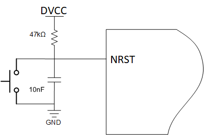
GUID-21990BBC-D6F6-463A-B062-D19C2E7E3966-low.png Figure 3-1 NRST Recommended Circuit