SLAAEG4 October   2023 MSPM0C1104 , MSPM0L1306


  1.   1
  2.   Abstract
  3.   Trademarks
  4. MSPM0C Hardware Design Check List
  5. Power Supplies in MSPM0C Devices
    1. 2.1 Digital Power Supply
    2. 2.2 Analog Power Supply
    3. 2.3 Built-in Power Supply and Voltage Reference
    4. 2.4 Recommended Decoupling Circuit for Power Supply
  6. Reset and Power Supply Supervisor
    1. 3.1 Digital Power Supply
    2. 3.2 Power Supply Supervisor
      1. 3.2.1 Power-On Reset (POR) Monitor
      2. 3.2.2 Brownout Reset (BOR) Monitor
      3. 3.2.3 POR and BOR Behavior During Supply Changes
  7. Clock System
    1. 4.1 Internal Oscillators
      1. 4.1.1 Internal Low-Frequency Oscillator (LFOSC)
      2. 4.1.2 Internal System Oscillator (SYSOSC)
    2. 4.2 External Clock Input (xFCLK_IN)
      1. 4.2.1 LFCLK_IN
      2. 4.2.2 HFCLK_IN
    3. 4.3 External Clock Output (CLK_OUT)
    4. 4.4 Frequency Clock Counter (FCC)
  8. Debugger
    1. 5.1 Debug Port Pins and Pinout
    2. 5.2 Debug Port Connection With Standard JTAG Connector
      1. 5.2.1 Standard XDS110
      2. 5.2.2 Lite XDS110 (MSPM0 LaunchPad™ kit)
  9. Key Analog Peripherals
    1. 6.1 ADC Design Considerations
  10. Key Digital Peripherals
    1. 7.1 Timer Resources and Design Considerations
    2. 7.2 UART and LIN Resources and Design Considerations
    3. 7.3 I2C and SPI Design Considerations
  11. GPIOs
    1. 8.1 GPIO Output Switching Speed and Load Capacitance
    2. 8.2 GPIO Current Sink and Source
    3. 8.3 Open-Drain GPIOs Enable 5-V Communication Without a Level Shifter
    4. 8.4 Communicate With 1.8-V Devices Without a Level Shifter
    5. 8.5 Unused Pins Connection
  12. Layout Guides
    1. 9.1 Power Supply Layout
    2. 9.2 Considerations for Ground Layout
      1. 9.2.1 What is Ground Noise?
    3. 9.3 Traces, Vias, and Other PCB Components
    4. 9.4 How to Select Board Layers and Recommended Stack-up
  13. 10References

External Clock Output (CLK_OUT)

A clock output unit is provided for pushing out digital clocks from the device to external circuits or to the frequency clock counter. This feature is useful for clocking external circuitry such as an external ADC that does not have its own clock source. The clock output unit has a flexible set of sources to select from and includes a programmable divider.
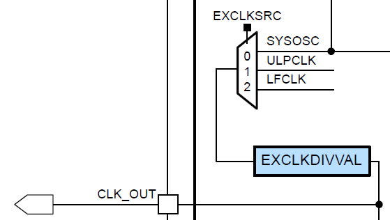
GUID-87997E35-C73F-41D3-B55B-9134805F2233-low.png Figure 4-4 MSPM0C Series External Clock Output

Available clock sources for CLK_OUT:

  • SYSOSC
  • ULPCLK
  • LFCLK

The selected clock source is divided by 2, 4, 6, 8, 10, 12, 14, or 16 before being output to the pin or to the frequency clock counter.