SLAAEG4 October 2023 MSPM0C1104 , MSPM0L1306
9.1 Power Supply Layout
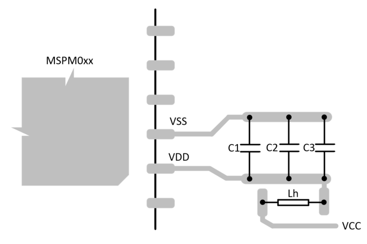
Figure 9-1 shows the typical parts placement and routing for the power supply
layout; you must modify this appropriately for your MSPM0C part. You can optionally
connect a filter inductor in series with the VCC and MCU VDD pins. This inductor is used
to filter the switching noise frequency of DCDC. For the value, refer to the data sheet
of DCDC vendor. C1, C2, and C3 values and layout in the MSPM0C device data sheets.
 Figure 9-1 Suggested Power Supply
Layout
Note:
- Keep the smallest capacitance, closest to the MCU VDD pin (C1 < C2 < C3).
- All the traces should be direct without any vias.
 Figure 9-1 Suggested Power Supply
Layout