SLAAEG4 October 2023 MSPM0C1104 , MSPM0L1306
9.3 Traces, Vias, and Other PCB Components
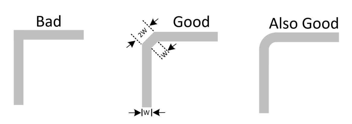
A right angle in a trace can cause more radiation. The capacitance increases in the region of the corner and the characteristic impedance changes. This impedance change causes reflections. Avoid right-angle bends in a trace and try to route them with at least two 45° corners. To minimize any impedance change, the best routing would be a round bend, as shown in Figure 9-3.
 Figure 9-3 Poor and Correct Way of
Bending Traces in Right Angle
Figure 9-3 Poor and Correct Way of
Bending Traces in Right AngleTo minimize crosstalk, not only between two signals on one layer but also between adjacent layers, route them 90° to each other. More complex boards need to use vias while routing; however, care must be taken when using vias as they add additional inductance and capacitance, and reflections occur due to the change in the characteristic impedance. Vias also increase the trace length. When using differential signals, use vias in both traces or compensate the delay in the other trace as well.
For signal traces, pay more attention to the impact of high-frequency pulse signals, especially on relatively small analog signals (like sensor signals). Too many crossovers will couple the electromagnetic noise of the high-frequency signal to the analog signal, which will result in a low signal-to-noise ratio of the signal and affect the signal quality. Therefore, it is necessary to avoid crossing when designing. But if there is indeed an unavoidable intersection, it is recommended to intersect vertically to minimize the interference of electromagnetic noise. Figure 9-4 shows how to reduce this noise.
 Figure 9-4 Poor and Correct Cross Traces
for Analog and High-Frequency Signals