SLAAEG4 October   2023 MSPM0C1104 , MSPM0L1306


  1.   1
  2.   Abstract
  3.   Trademarks
  4. MSPM0C Hardware Design Check List
  5. Power Supplies in MSPM0C Devices
    1. 2.1 Digital Power Supply
    2. 2.2 Analog Power Supply
    3. 2.3 Built-in Power Supply and Voltage Reference
    4. 2.4 Recommended Decoupling Circuit for Power Supply
  6. Reset and Power Supply Supervisor
    1. 3.1 Digital Power Supply
    2. 3.2 Power Supply Supervisor
      1. 3.2.1 Power-On Reset (POR) Monitor
      2. 3.2.2 Brownout Reset (BOR) Monitor
      3. 3.2.3 POR and BOR Behavior During Supply Changes
  7. Clock System
    1. 4.1 Internal Oscillators
      1. 4.1.1 Internal Low-Frequency Oscillator (LFOSC)
      2. 4.1.2 Internal System Oscillator (SYSOSC)
    2. 4.2 External Clock Input (xFCLK_IN)
      1. 4.2.1 LFCLK_IN
      2. 4.2.2 HFCLK_IN
    3. 4.3 External Clock Output (CLK_OUT)
    4. 4.4 Frequency Clock Counter (FCC)
  8. Debugger
    1. 5.1 Debug Port Pins and Pinout
    2. 5.2 Debug Port Connection With Standard JTAG Connector
      1. 5.2.1 Standard XDS110
      2. 5.2.2 Lite XDS110 (MSPM0 LaunchPad™ kit)
  9. Key Analog Peripherals
    1. 6.1 ADC Design Considerations
  10. Key Digital Peripherals
    1. 7.1 Timer Resources and Design Considerations
    2. 7.2 UART and LIN Resources and Design Considerations
    3. 7.3 I2C and SPI Design Considerations
  11. GPIOs
    1. 8.1 GPIO Output Switching Speed and Load Capacitance
    2. 8.2 GPIO Current Sink and Source
    3. 8.3 Open-Drain GPIOs Enable 5-V Communication Without a Level Shifter
    4. 8.4 Communicate With 1.8-V Devices Without a Level Shifter
    5. 8.5 Unused Pins Connection
  12. Layout Guides
    1. 9.1 Power Supply Layout
    2. 9.2 Considerations for Ground Layout
      1. 9.2.1 What is Ground Noise?
    3. 9.3 Traces, Vias, and Other PCB Components
    4. 9.4 How to Select Board Layers and Recommended Stack-up
  13. 10References

How to Select Board Layers and Recommended Stack-up

To reduce the reflections on high speed signals, it is necessary to match the impedance between the source, sink and transmission lines. The impedance of a signal trace depends on its geometry and its position with respect to any reference planes.

The trace width and spacing between differential pairs for a specific impedance requirement is dependent on the chosen PCB stack-up. As there are limitations in the minimum trace width and spacing which depend on the type of PCB technology and cost requirements, a PCB stack-up needs to be chosen which allows all the required impedances to be realized.

The minimum configuration that can be used is 2 stack-up. A 4- or 6-layer boards is required for very dense PCBs that have multiple high-speed signals.

The following stack-up (see Figure 9-5) is a 4-layer examples that can be used as a starting point for helping in a stack-up evaluation and selection. These stack-up configurations are using a GND plane adjacent to the power plane to increase the capacitance and reduce the gap between GND and power plane. So high speed signals on top layer will have a solid GND reference plane which helps to reduce EMC emissions, as going up in number of layers and having a GND reference for each PCB signal layer will improve further the radiated EMC performance.
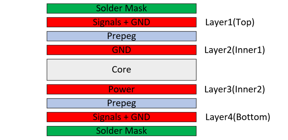
GUID-7AE0DFD3-E138-40E3-9AB5-28033C683D3F-low.png Figure 9-5 Four-Layer PCB Stack-up Example

If the system is not very complicated, there is no high-speed signal or some sensitive analog signal, then the 2 stack-up structure is sufficient.