SLAAEI9 December   2023 MSPM0C1103 , MSPM0C1104 , MSPM0C1104-Q1 , MSPM0G1105 , MSPM0G1106 , MSPM0G1107 , MSPM0G1505 , MSPM0G1506 , MSPM0G1507 , MSPM0G3105 , MSPM0G3105-Q1 , MSPM0G3106 , MSPM0G3106-Q1 , MSPM0G3107 , MSPM0G3107-Q1 , MSPM0G3505 , MSPM0G3505-Q1 , MSPM0G3506 , MSPM0G3506-Q1 , MSPM0G3507 , MSPM0G3507-Q1 , MSPM0L1105 , MSPM0L1106 , MSPM0L1228


  1.   1
  2.   Abstract
  3.   Trademarks
  4. 1MSPM0 Portfolio Overview
    1. 1.1 Introduction
    2. 1.2 Portfolio Comparison of STM8 MCUs to MSPM0 MCUs
  5. 2Ecosystem And Migration
    1. 2.1 Ecosystem Comparison
      1. 2.1.1 MSPM0 Software Development Kit (MSPM0 SDK)
      2. 2.1.2 The IDE Supported By MSPM0
      3. 2.1.3 SysConfig
      4. 2.1.4 Debug Tools
      5. 2.1.5 LaunchPad
    2. 2.2 Migration Process
      1. 2.2.1 Step 1. Choose The Right MSPM0 MCU
      2. 2.2.2 Step 2. Set Up IDE And Quick Introduction of CCS
        1. 2.2.2.1 Set Up IDE
        2. 2.2.2.2 Quick Introduction of CCS
      3. 2.2.3 Step 3. Set Up MSPM0 SDK And Quick Introduction of MSPM0 SDK
        1. 2.2.3.1 Set Up MSPM0 SDK
        2. 2.2.3.2 Quick Introduction of SDK
      4. 2.2.4 Step 4. Software Evaluation
      5. 2.2.5 Step 5. PCB Board Design
      6. 2.2.6 Step 6. Mass Production
    3. 2.3 Example
  6. 3Core Architecture Comparison
    1. 3.1 CPU
    2. 3.2 Embedded Memory Comparison
      1. 3.2.1 Flash and EEPROM Features
      2. 3.2.2 Flash and EEPROM Organization
        1. 3.2.2.1 Flash and EEPROM Regions
        2. 3.2.2.2 NONMAIN Memory of MSPM0
      3. 3.2.3 Embedded SRAM
    3. 3.3 Power UP and Reset Summary and Comparison
    4. 3.4 Clocks Summary and Comparison
      1. 3.4.1 Oscillators
      2. 3.4.2 Clock Signal Comparison
    5. 3.5 MSPM0 Operating Modes Summary and Comparison
      1. 3.5.1 Operating Modes Comparison
      2. 3.5.2 MSPM0 Capabilities in Lower Modes
      3. 3.5.3 Entering Lower-Power Modes
      4. 3.5.4 Low-Power Mode Code Examples
    6. 3.6 Interrupts and Events Comparison
      1. 3.6.1 Interrupts and Exceptions
        1. 3.6.1.1 Interrupt Management of MSPM0
        2. 3.6.1.2 Interrupt Controller (ITC) of STM8
      2. 3.6.2 Event Handler of MSPM0
      3. 3.6.3 Event Management Comparison
    7. 3.7 Debug and Programming Comparison
      1. 3.7.1 Debug Mode Comparison
      2. 3.7.2 Programming Mode Comparison
        1. 3.7.2.1 Bootstrap Loader (BSL) Programming Options
  7. 4Digital Peripheral Comparison
    1. 4.1 General-Purpose I/O (GPIO, IOMUX)
    2. 4.2 Universal Asynchronous Receiver-Transmitter (UART)
    3. 4.3 Serial Peripheral Interface (SPI)
    4. 4.4 Inter-integrated Circuit Interface (I2C)
    5. 4.5 Timers (TIMGx, TIMAx)
    6. 4.6 Windowed Watchdog Timer (WWDT)
  8. 5Analog Peripheral Comparison
    1. 5.1 Analog-to-Digital Converter (ADC)
    2. 5.2 Comparator (COMP)
    3. 5.3 Voltage References (VREF)

Power UP and Reset Summary and Comparison

Both STM8 devices and MSPM0 devices have the minimum operating voltage and have modules in place to make sure that the device starts up properly by holding the device or portions of the device in a reset state. Table 3-5 shows a comparison on how this is done between the two families and what modules control the power up process and reset across the families.

Table 3-5 Summary and Comparison of Power Up
STM8 MSPM0
Power-On Reset (POR) Rise detection: VDD>VPOR, POR state is released, BOR starts to work. Power-On Reset (POR) Rise detection: VDD>POR+, POR state is released, and bandgap reference and BOR is started
Fall detection: VDD<POR-, device is held in POR state
Power-Down Reset (PDR) Fall detection: VDD<VPDR, PDR keeps the device under reset.
Brownout Reset (BOR)(1) Rise detection: VDD>VBOR+, BOR state is released, device continues the boot process.
Fall detection: VDD<VBOR-, BOR state is generated.
BOR has five different levels to be selected.
Brownout Reset (BOR)- 0 level(2) Rise detection: VDD>BOR0+,
Device continues the boot process, and PMU is started
Fall detection: VDD<BOR0-,
Device is held in BOR state.
Brownout Reset (BOR)- 1 to 3 level(2) Fall detection:
1) VDD<BORx- (x=1, 2, 3), an interrupt request is generated, and the BOR circuit automatically switches the BOR threshold level to BOR0.
2) VDD<BOR0-, Device is held in BOR state
Programmable voltage detector (PVD)(3) Rise detection: VDD>VPVD, a PVD event is genrated.
Fall detection: VDD<VPVD, a PVD event is genrated. PVD has seven different levels to be selected.
N/A N/A
RTC Reset RTC and associated registers are reset through system reset or power-on reset. RTC Reset RTC and associated clocks are reset through BOOTRST, BOR, or POR
During startup, the BOR need be configued to BOR Level 0 to make sure the minimum operating voltage. BOR is always active at power-on, keeping the MCU under reset till the application operating threshold is reached. If the BOR is disabled at power-down, the reset threshold is VPDR to make sure a VDD min.
There are four selectable BOR threshold levels (BOR0-BOR3). During startup, the BOR threshold is always BOR0 (the lowest value) to make the device always starts at the specified VDD minimum. After boot, software can optionally re-configure the BOR circuit to use a different (higher) threshold level.
STM8L001xx, STM8L101xx and STM8S series microcontrollers don't have the PVD.

Figure 3-1 shows the MSPM0 Reset function. MSPM0 devices have five reset levels: Power-on reset (POR), Brownout reset (BOR), Boot reset (BOOTRST), System reset (SYSRST) and CPU reset (CPURST).
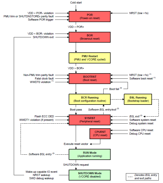
GUID-0FB084DB-B2BB-4932-AF37-1E0737C021CB-low.png Figure 3-1 MSP Reset Function