SLAAEL5 August 2024 AFE539F1-Q1
Introduction
 Figure 1 Simplified Block Diagram of a Traction Inverter
The DC-Link capacitor is a part of every traction inverter and is positioned in parallel with the high-voltage battery and the power stage (see Figure 1). The DC-Link capacitor has several functions, such as to help smooth voltage ripples, filtering unwanted harmonics and reducing noise.
To provide operational safety, the DC-Link capacitor must be discharged in two distinct operational scenarios: normal operation, such as after turning off the vehicle, and emergency situations, like post-vehicle collision or dangerous fault scenarios during maintenance. This discharge process aims to safeguard occupants or maintenance personnel, minimizing the risk of personal injury from contact with live components or potential fire hazards. Depending on the safety assessment of the manufacturer this application is often rated as ASIL-B.
This application brief emphasizes the emergency operation with the subsequent content describing the norm. With a nominal battery voltage of 800VDC, this electrical circuit falls under voltage class B, categorized with a range of 60V < VDC ≤ 1500V. ISO 6469 Part 4 mandates that bus voltage must reach and remain below 60VDC within 5 seconds in the worst-case scenario, following the moment the vehicle comes to a halt after a collision.
There are multiple ways to do active discharge using the existing components in the system. Some system designers use the power stage or motor windings as dissipation element, which is controlled by an MCU for a constant discharge. The safety assessment of some manufacturers does not permit using these methods due to concerns about premature degradation of life and the dependency of an MCU. Hence, a separate circuit is frequently added to address these concerns.
The AFE539F1-Q1 serves as an analog front end designed for active discharge applications. The device features a 10-bit analog-to-digital converter (ADC) input and a 7-bit pulse-width-modulation (PWM) output. This part contains an integrated state machine with a preprogrammed constant power dissipation control and acts as a Voltage-to-PWM converter. Therefore, the device allows discharge of the DC-Link capacitor without the need of an MCU. Incorporating TI's AFE539F1-Q1 aims to lower the overall BOM costs, reduce weight and size targeting the power resistor in comparison to the commonly-used design (see Legacy method: Brute force discharge).
Table 1 outlines the typical specification, which is the system assumptions of this brief. These specifications can vary depending on the safety concept of the traction inverter manufacturer.
| Parameter | Specification |
|---|---|
| Maximum voltage of capacitor | 1000VDC |
| Safe voltage threshold | 60VDC |
| Capacitor size | 1mF |
| Dissipation time | < 5s |
| BMS disconnected | Yes |
Legacy Method: Brute Force Discharge
Figure 2 shows a typical implementation for DC-Link capacitor discharge circuits. When the DC-Link capacitor is disconnected from any power source, an activated power switch dissipates the remaining energy through the power resistor Rload. This method is straightforward and effective for low-power applications where the expense of the power resistor does not greatly impact the overall bill of material (BOM). However, this is not the case for applications involving high voltage and substantial power dissipation. With up to 85% share, the cost of the power resistor becomes a significant portion of the BOM.
 Figure 2 Legacy Brute Force Method Using the TPSI3050-Q1
Figure 2 illustrates a simplified block diagram of the legacy brute-force method. The design uses the TPSI3050-Q1 as gate driver with the primary power supply fed in through the EN pin.
A capacitor discharges negatively exponentially which is described in Equation 1:
where
- U0 = Initial capacitor voltage in V
- C = DC-Link capacitance in F
- R = Rload resistance in Ω
With the given system assumptions, the resistor size can be calculated as Equation 2 shows.
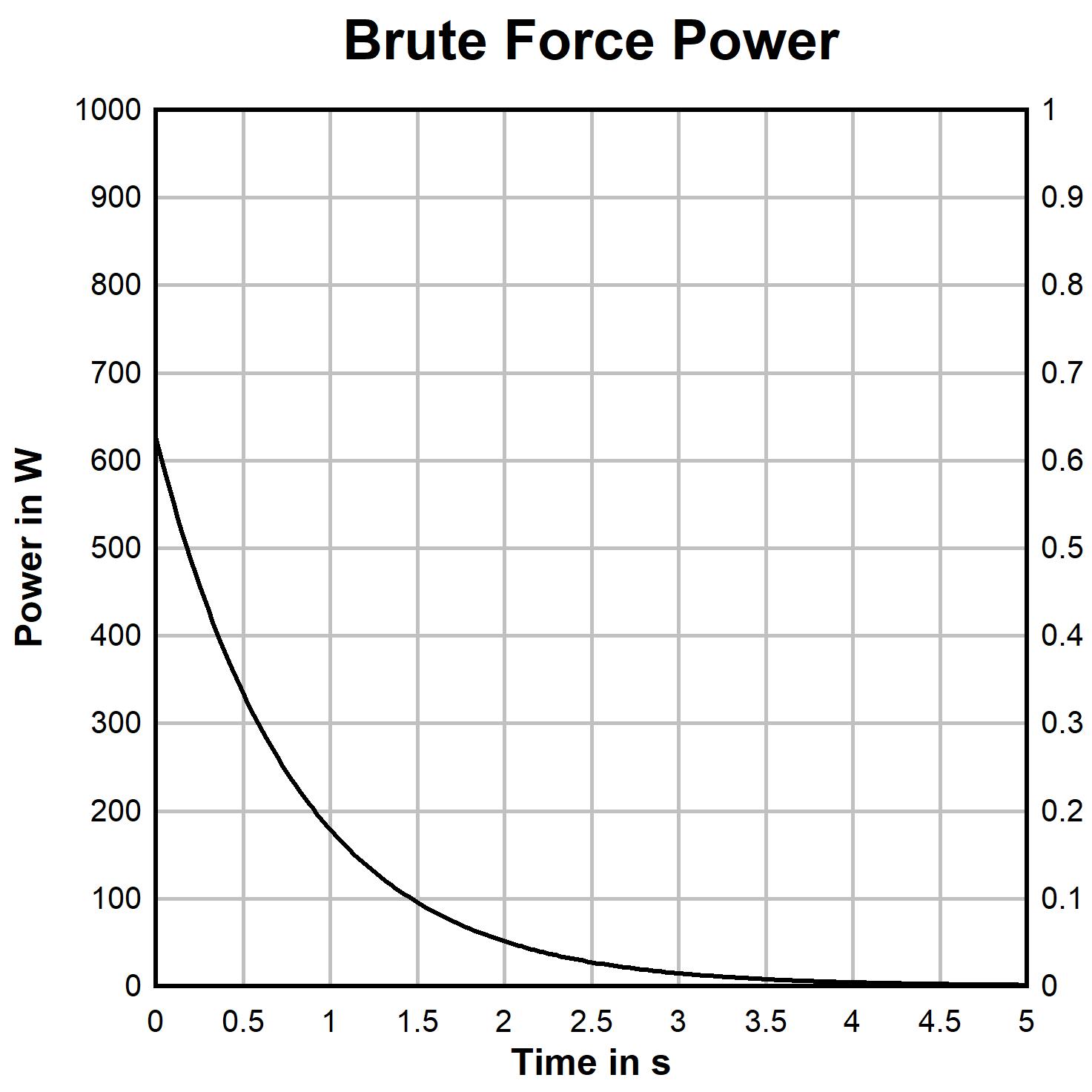
With 1600Ω as the closest standard resistor value, the circuit reaches 60VDC within 4.5 seconds. Using Ohm’s Law, the peak current is 625mA. Consequently, the power resistor must have a power rating of 625W, (see Figure 3 power at t = 0 seconds). This considers that the discharging circuit is used on a frequent basis, therefore Rload is not damaged and the surrounding board area does not overheat. If this circuit is only used as a backup emergency discharge, the resistor has enough cool-down time in between usage. Therefore, an overload condition of the power resistor can be considered.
 Figure 3 Power Distribution Over Time With Brute Force
Using PWM for Constant Power Dissipation
By using a resistor as a thermal dissipation element the power rating is the main cost, weight, and size driver for the resistor. The power curve in Figure 3 shows that the power dissipation naturally decreases exponentially.
 Figure 4 Changing the Effective Resistance
To distribute the power dissipation more evenly, a low-side switch changes the effective resistance Reff by applying different duty cycles to this circuit. (see Figure 4 and Equation 3).
where
- D = Duty cycle with 0 ≤ D ≤ 1
The AFE539F1-Q1 device essentially acts as a Voltage-to-PWM converter. This allows low duty cycle, therefore higher resistance in the early discharge stages. An increasing duty cycle over time gradually lowers the resistance to Rload. The configuration is programmed individually in a non-volatile memory, which incorporates the discharge curve. Hence, after this circuit is activated the circuit can run locally and without the need of an additional MCU.
When it comes to the system view there are a few benefits of discharging the DC-Link capacitor with constant power dissipation. The first benefit, as previously elaborated, is the wattage of the power resistor. Secondly, this directly applies to the respective heat sink either procured separately or integrated. With a constant high temperature, the full thermal capacity is taken advantage of for the whole discharging time rather than sizing the heat sink for the worst case of early discharging phases. Furthermore, an evenly-distributed current and heat dissipation over time can enhance the lifetime of devices which are directly used (for example, power switch or shunt) or devices which physically surround the circuit.
The resistive active discharge circuit is implemented on the high-voltage side, also called the hot side or power board. By sensing the bus voltage, the AFE539F1-Q1 outputs different PWM signals to the gate driver, which is responsible for the power switch. The UCC27531-Q1 is a simple and cost-sensitive single gate driver, which opens up the possibility to either drive IGBTs, Si-FETs, or SIC-FETs. Since the AFE539F1-Q1 requires the measured DC-Link voltage as an input value, there is a need for a resistor divider. To save space to a comparably long resistor chain and to limit the drift over lifetime, a highly-accurate RES60A-Q1 divider is recommended. The circuit can be activated by using the EN pin of the gate driver UCC27531-Q1. A digital isolator device ISO6721-Q1 is used to transfer the enable signal from the low-voltage side, which can be triggered either by MCU, a supervisor, or any fail-safe logic.
Usually the DC-Link capacitor discharge is tested with every start-up to provide the functionality. To avoid extensive usage of the battery connecting relay, the current can be sensed with a shunt. Either an operational amplifier LM2904B-Q1 or an instrumentation amplifier can be used. The current signal can be transferred to the low-voltage side, using the same bidirectional digital isolator ISO6721-Q1. This monitoring allows implementation of diagnostic features in the system.
 Figure 5 Constant Power Dissipation With PWM Using AFE539F1-Q1
Calculations and Configuration
This section describes how to perform calculation on the active discharge circuit, which can be adapted to different system specifications.
The AFE539F1-Q1 has a configuration parameter which can be configured through the serial peripheral interface (SPI) or I²C. With the respective evaluation board these values can be changed easily with the user interface SMART-DAC-EVM-GUI.
- PWM Frequency (1.017kHz or 0x0B): With higher frequencies issues can occur with parasitic inductances
- Reference Gain (1 ×, VDD as reference): High full scale with easy implementation
Function Coefficient (K = 0x186): required to reach system requirements of 5 seconds (See Table 1)
- Minimum Duty Cycle (0x00 ) and Maximum Duty Cycle (0x7F ): Usage of full duty cycle range from 0% to 100%
To calculate the ADC-input of the AFE539F1-Q1, the full-scale voltage has to be defined using the data in Table 2. The design goal is to have a large full-scale range. With a VDD = 5V, the full scale is defined by VFS = 5/3V. With Vbus = 1000V, the resistor divider ratio is approximately 599:1. RES60A-Q1 has a nominal resistance of 12.5MΩ and a built-in ratio of 610:1.
| Reference Input | Operational Range | Gain | VFS (Internally Divided by 3) |
|---|---|---|---|
| Power Supply | 1.7V–5.5V | 1 × | 0.567V–1.833V |
| External | 1.7V–5.5V | 1 × | 0.567V–1.833V |
| Internal | 1.1979V–1.224V | 1.5 × | 0.599V–0.612V |
| 2 × | 0.799V–0.816V |
Now that the full-scale voltage VFS is set, the ADC input is defined as an integer in Equation 5.
where
- VIN = ADC input with VIN = Vbus * resistor divider ratio
- VFS = ADC full scale defined by AFE539F1-Q1 configurations
- N = ADC-resolution = 8-bit
Equation 6 shows how the duty cycle is calculated, depending on the configurable value K.
where
- PWM Code = Defined as integer from 1 to 127
- K = Configuration value from 0 to 65535
Combining Equation 5 and Equation 6 results in the final Equation 7. Use Equation 8 to calculate the actual duty cycle.
Again, putting these equations together, the function D (VIN) determines duty cycle change depending on the voltage threshold. For PWM code = 127 the duty cycle is forced to 100%.
| PWM Code | Duty Cycle | From Vbus | To Vbus |
|---|---|---|---|
| 1 | 0.78% | 1000V | 628.52V |
| 2 | 1.56% | 628.52V | 512.98V |
| 3 | 2.34% | 512.98V | 445.38V |
| 4 | 3.13% | 445.38V | 397.66V |
| … | … | … | … |
| 127 | 100% | 79.53V |
With these thresholds and remembering the negative exponential capacitor discharge in Equation 1, Figure 6 shows how the DC-Link capacitor is discharged over time. With every duty cycle step the effective resistance changes, which creates a different graph section.
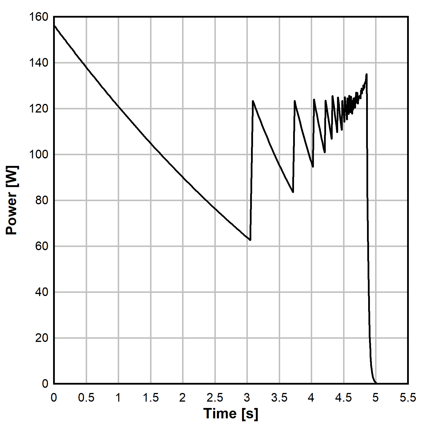
To choose a power resistor and K, while still meeting the system requirements a calculation sheet is provided along with the AFE539F1-Q1. Wirewound resistors tend to have high parasitic inductances which can lead to increased slew rates. Therefore, thick film resistors are a recommended choice coupled with a low switching frequency. Figure 7 illustrates the evenly-calculated power dissipation.
 Figure 6 DC-Link Voltage Over Time With K = 390, Vbus = 1000V, Ratio 610:1 and Rload = 50Ω
 Figure 7 Power Dissipation Over Time With
K = 390, Vbus = 1000V, Ratio 610:1 and Rload = 50Ω
Conclusion
When choosing with K = 390, Vbus = 1000V, resistor ratio 610:1, and Rload = 50Ω this concludes a power dissipation shown in Figure 7. This setup can discharge the DC-Link capacitor within 4.9 seconds and a peak power of about 160W. The respective spikes, also in current are occurring with every duty cycle step change. An equally fast dissipation without PWM needs a power resistor rating of around 625W. For this circuit the power resistor can have a BOM share of up to 85%. In conclusion the reduction of the power rating from 625W to 160W can lead to cost benefits of up to 50%.