SLAAEO3 September   2024 MSPM0L1227 , MSPM0L1228 , MSPM0L1228-Q1 , MSPM0L2227 , MSPM0L2228 , MSPM0L2228-Q1


  1.   1
  2.   Abstract
  3.   Trademarks
  4. 1Introduction: MSPM0 and LCD End Applications
  5. 2MSPM0 LCD Portfolio
  6. 3Segmented LCD Operation
    1. 3.1 LCD Structure (Simplified)
    2. 3.2 LCD Drive Basics
  7. 4MSPM0 LCD Features
    1. 4.1 Muxing
      1. 4.1.1 Muxing Example
    2. 4.2 Voltage Generation
      1. 4.2.1 Charge Pump
      2. 4.2.2 Contrast Control
    3. 4.3 LCD Clocking
    4. 4.4 LCD Memory and Blinking Mode
      1. 4.4.1 LCD Memory Organization
      2. 4.4.2 Blinking
    5. 4.5 LCD Output Pin Configuration
    6. 4.6 Low Power Mode Feature
  8. 5LCD Layout and Software Considerations
    1. 5.1 LCD Layout Tips
      1. 5.1.1 Hardware-Driven Layout
      2. 5.1.2 Software-Driven Layout
      3. 5.1.3 General Layout Rules
    2. 5.2 LCD Software Tips
      1. 5.2.1 Create a Look-up Table
      2. 5.2.2 Use of #defines
      3. 5.2.3 Efficient Clearing of the LCD Memory
      4. 5.2.4 Double-buffering of the Display Buffer Using Dual Display Memory
  9. 6Additional Resources

Hardware-Driven Layout

In a hardware-driven layout approach, one option is for pins to be connected to the closest LCD-capable pins on the MSPM0 to minimize crossings and layout the board in a single layer. However, the hardware-driven approach in layouts where the pins mapped to the MSPM0 LCD memory are scattered through memory, meaning more software work and overhead when writing the code.
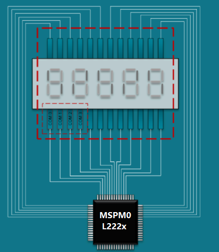
MSPM0L222x Example Layout Grouping LCD
                    Lines Bus-Style in a Single Layer Figure 5-2 Example Layout Grouping LCD Lines Bus-Style in a Single Layer