• Menu
  • Product
  • Email
  • PDF
  • Order now
  • MSPM0 ADC Noise Analysis and Application

    • SLAAEO8 October   2024 MSPM0C1103 , MSPM0C1103-Q1 , MSPM0C1104 , MSPM0C1104-Q1 , MSPM0C1106 , MSPM0C1106-Q1 , MSPM0G1105 , MSPM0G1106 , MSPM0G1107 , MSPM0G1505 , MSPM0G1506 , MSPM0G1507 , MSPM0G1518 , MSPM0G1519 , MSPM0G3105 , MSPM0G3105-Q1 , MSPM0G3106 , MSPM0G3106-Q1 , MSPM0G3107 , MSPM0G3107-Q1 , MSPM0G3505 , MSPM0G3505-Q1 , MSPM0G3506 , MSPM0G3506-Q1 , MSPM0G3507 , MSPM0G3507-Q1 , MSPM0G3518 , MSPM0G3519 , MSPM0G3519-Q1 , MSPM0H3216 , MSPM0H3216-Q1 , MSPM0L1105


  • CONTENTS
  • SEARCH
  • MSPM0 ADC Noise Analysis and Application
  1.   1
  2.   Abstract
  3.   Trademarks
  4. 1ADC Introduction
    1. 1.1 SAR ADC Principle
    2. 1.2 ADC Parameters
      1. 1.2.1 Static Parameters
      2. 1.2.2 Dynamic Parameters
        1. 1.2.2.1 AC Parameters
        2. 1.2.2.2 DC Parameters
  5. 2ADC Noise Analysis
    1. 2.1 ADC Noise Classification
      1. 2.1.1 ADC Noise
      2. 2.1.2 Reference Noise
      3. 2.1.3 Power Supply Noise
      4. 2.1.4 ADC Input Noise
      5. 2.1.5 Clock Jitter
    2. 2.2 How to Reduce Noise
      1. 2.2.1 Reducing Input Noise Through RC Filtering
      2. 2.2.2 Layout Suggestions
      3. 2.2.3 Improving Signal-to-Noise Ratio
      4. 2.2.4 Choose a Suitable Reference Voltage Source
      5. 2.2.5 Software Methods for Reducing Noise
  6. 3ADC Oversampling
    1. 3.1 Sampling Rate
    2. 3.2 Extraction
    3. 3.3 Application Conditions
  7. 4ADC Application Based on MSPM0
    1. 4.1 ADC Configuration of MSPM0
    2. 4.2 ADC DC Test Based on MSPM0G3507 ADC EVM Board
      1. 4.2.1 Software/Hardware Configuration
        1. 4.2.1.1 Hardware
        2. 4.2.1.2 Software
      2. 4.2.2 Test Result
      3. 4.2.3 Result Analysis and Conclusion
  8. IMPORTANT NOTICE
search No matches found.
  • Full reading width
    • Full reading width
    • Comfortable reading width
    • Expanded reading width
  • Card for each section
  • Card with all content


Application Note

MSPM0 ADC Noise Analysis and Application

Abstract

This document provides analog-to-digital converter (ADC) noise analysis and introduces the MSPM0 MCU ADC application.

Trademarks

All trademarks are the property of their respective owners.

1 ADC Introduction

1.1 SAR ADC Principle

Figure 1-1 shows the system schematic diagram of SAR ADC. SAR ADC controls the switching of multiple switches (12 switches in this case) to perform capacitive voltage division on VREF and obtain different analog voltage output results. Compare the analog voltage with the input sampling signal, and the output of the comparator is used to adjust the on/off state of the switch, ultimately making the simulated voltage obtained by VREF voltage division as close as possible to the input voltage. The actual comparison process is achieved by using the binary method to approximate VREF division for the VIN, thus requiring 12 cycles for data conversion. When considering the ADC triggering, signal sampling and holding time, the actual SAR ADC conversion process takes more than 12 cycles (It takes 14 conversion cycles in MSPM0 G-Series).
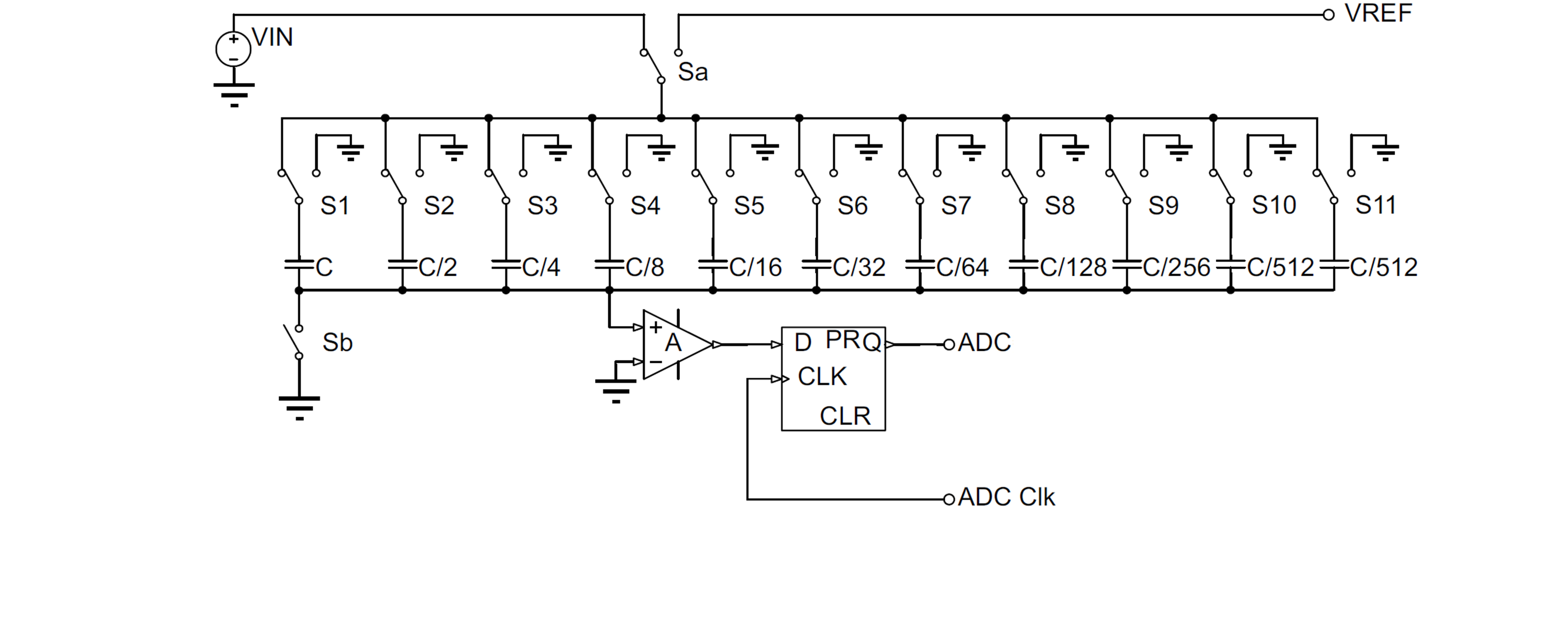

 Principle Block Diagram of SAR
                    ADC Based on CDAC

Figure 1-1 Principle Block Diagram of SAR ADC Based on CDAC


Texas Instruments

© Copyright 1995-2025 Texas Instruments Incorporated. All rights reserved.
Submit documentation feedback | IMPORTANT NOTICE | Trademarks | Privacy policy | Cookie policy | Terms of use | Terms of sale