SLAAEO8 October 2024 MSPM0C1103 , MSPM0C1103-Q1 , MSPM0C1104 , MSPM0C1104-Q1 , MSPM0G1105 , MSPM0G1106 , MSPM0G1107 , MSPM0G1505 , MSPM0G1506 , MSPM0G1507 , MSPM0G1519 , MSPM0G3105 , MSPM0G3105-Q1 , MSPM0G3106 , MSPM0G3106-Q1 , MSPM0G3107 , MSPM0G3107-Q1 , MSPM0G3505 , MSPM0G3505-Q1 , MSPM0G3506 , MSPM0G3506-Q1 , MSPM0G3507 , MSPM0G3507-Q1 , MSPM0G3519 , MSPM0L1105
1.2.2.2 DC Parameters
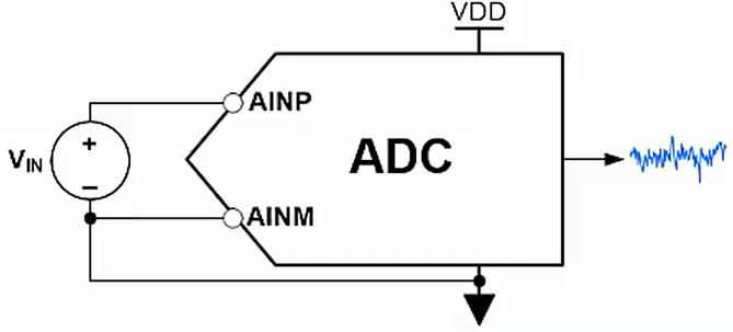
Measurement conditions: Connect a constant DC voltage between the positive and negative terminals of the ADC input, and observe the distribution of the output digital results.
 Figure 1-3 Schematic Diagram of ADC DC
Test
Figure 1-3 Schematic Diagram of ADC DC
TestIn theory, when the quantity of the sampled data is large enough, the noise superimposed on the DC signal approximates a normal distribution. The effective value of noise is the standard deviation σ of the data sample. The probability of data distribution within the range of u-3σ~u+3σ is 99.73%, so the peak to peak value of a DC signal is approximately 6σ.
- Effective Resolution
The effective resolution of ADC under DC input can be obtained by dividing the full-scale range (FSR) of ADC by the effective value of noise and taking the logarithm of 2. This resolution is of great significance in DC signal sampling scenarios or low-frequency signal sampling scenarios, and can reflect the effective number of ADC digital results in practical applications.
Equation 9.The above formula represents the effective resolution calculation method when the DC input is at full scale. When the input is not at full scale, the calculation formula is modified to:
Equation 10.That is to say, the effective resolution is related to the voltage input. In theory, the larger the input voltage, the higher the DC effective resolution. Therefore, for small input signals, they are usually amplified to close to FSR through a preamplifier, to get a large effective resolution. It should be noted that the amplified noise (1/f noise and broadband band noise) should not be introduced too much.
- Noise-free resolution
By dividing the full range of ADC by the peak to peak value of noise and taking the logarithm of the two, the noise free resolution of ADC under DC input can be obtained. It reflects the number of digits bit that can maintains stability under constant input.
Equation 11.