SLAAEO8 October 2024 MSPM0C1103 , MSPM0C1103-Q1 , MSPM0C1104 , MSPM0C1104-Q1 , MSPM0G1105 , MSPM0G1106 , MSPM0G1107 , MSPM0G1505 , MSPM0G1506 , MSPM0G1507 , MSPM0G3105 , MSPM0G3105-Q1 , MSPM0G3106 , MSPM0G3106-Q1 , MSPM0G3107 , MSPM0G3107-Q1 , MSPM0G3505 , MSPM0G3505-Q1 , MSPM0G3506 , MSPM0G3506-Q1 , MSPM0G3507 , MSPM0G3507-Q1 , MSPM0G3519 , MSPM0L1105
2.1 ADC Noise Classification
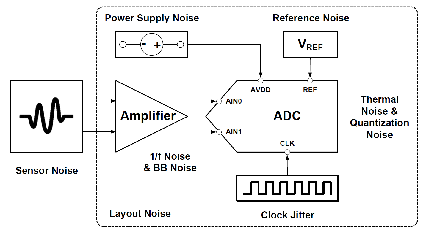
The following figure shows the block diagram of an ADC system, which shows the signal chain of ADC sampling data and the necessary signal inputs for the operation of the ADC module. Each link may introduce noise to the ADC system, so the sources of ADC system noise include sensor noise, operational amplifier noise, ADC noise, power supply noise, reference voltage noise, and clock jitter noise.
The sensor noise and operational amplifier usage vary greatly depending on the application scenario, and are greatly affected by the layout. This article classifies them as input noise of the ADC. Figure 2-1introduces the sources of noise in each stage separately.
 Figure 2-1 Schematic Diagram of ADC Noise
Sources