SLAS898B January 2014 – April 2015 TAS2552
PRODUCTION DATA.
- 1 Features
- 2 Applications
- 3 Description
- 4 Revision History
- 5 Pin Configuration and Functions
- 6 Specifications
-
7 Detailed Description
- 7.1 Overview
- 7.2 Functional Block Diagram
- 7.3
Feature Description
- 7.3.1 General I2C Operation
- 7.3.2 Single-Byte and Multiple-Byte Transfers
- 7.3.3 Single-Byte Write
- 7.3.4 Multiple-Byte Write and Incremental Multiple-Byte Write
- 7.3.5 Single-Byte Read
- 7.3.6 Multiple-Byte Read
- 7.3.7 PLL
- 7.3.8 Gain Settings
- 7.3.9 Class-D Edge Rate Control
- 7.3.10 Battery Tracking AGC
- 7.3.11 Configurable Boost Current Limit (ILIM)
- 7.4 Device Functional Modes
- 7.5
Register Map
- 7.5.1 Register Map Summary
- 7.5.2 Register 0x00: Device Status Register
- 7.5.3 Register 0x01: Configuration Register 1
- 7.5.4 Register 0x02: Configuration Register 2
- 7.5.5 Register 0x03: Configuration Register 3
- 7.5.6 Register 0x04: DOUT Tristate Mode
- 7.5.7 Register 0x05: Serial Interface Control Register 1
- 7.5.8 Register 0x06: Serial Interface Control Register 2
- 7.5.9 Register 0x07: Output Data Register
- 7.5.10 Register 0x08: PLL Control Register 1
- 7.5.11 Register 0x09: PLL Control Register 2
- 7.5.12 Register 0x0A: PLL Control Register 3
- 7.5.13 Register 0x0B: Battery Tracking Inflection Point Register
- 7.5.14 Register 0x0C: Battery Tracking Slope Control Register
- 7.5.15 Register 0x0D: Reserved Register
- 7.5.16 Register 0x0E: Battery Tracking Limiter Attack Rate and Hysteresis Time
- 7.5.17 Register 0x0F: Battery Tracking Limiter Release Rate
- 7.5.18 Register 0x10: Battery Tracking Limiter Integration Count Control
- 7.5.19 Register 0x11: PDM Configuration Register
- 7.5.20 Register 0x12: PGA Gain Register
- 7.5.21 Register 0x13: Class-D Edge Rate Control Register
- 7.5.22 Register 0x14: Boost Auto-Pass Through Control Register
- 7.5.23 Register 0x15: Reserved Register
- 7.5.24 Register 0x16: Version Number
- 7.5.25 Register 0x17: Reserved Register
- 7.5.26 Register 0x18: Reserved Register
- 7.5.27 Register 0x19: VBAT Data Register
- 8 Applications and Implementation
- 9 Power Supply Recommendations
- 10Layout
- 11Device and Documentation Support
- 12Mechanical, Packaging, and Orderable Information
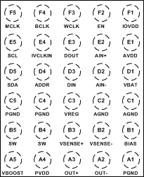
5 Pin Configuration and Functions
30-Ball WCSP
YFF Package
(Top View)

Pin Functions
| TERMINAL | INPUT/OUTPUT/POWER | DESCRIPTION | |
|---|---|---|---|
| NAME | BALL WCSP | ||
| PGND | A1 | P | Power ground. Connect to high current ground plane. |
| OUT– | A2 | O | Inverting Class D output. |
| OUT+ | A3 | O | Non-inverting Class D output. |
| PVDD | A4 | P | Class-D power supply. Connected internally to VBOOST – do not drive this terminal externally. |
| VBOOST | A5 | P | 8.5 V boost output. Connected internally to PVDD – do not drive this terminal externally. |
| BIAS | B1 | O | Mid-rail reference for Class D channel. |
| VSENSE– | B2 | I | Inverting voltage sense input. |
| VSENSE+ | B3 | I | Non-inverting voltage sense input. |
| SW | B4,B5 | I/O | Boost switch terminal. |
| AGND | C1,C2 | P | Analog ground. Connect to low noise ground plane. |
| VREG | C3 | O | High-side FET gate drive boost converter. |
| PGND | C4,C5 | P | Power ground. Connect to high current ground plane. |
| VBAT | D1 | P | Battery power supply. Connect to 3.0 V to 5.5 V battery supply. |
| AIN– | D2 | I | Inverting analog input. |
| DIN | D3 | I | Audio serial data input. Format is I2S, LJF, RJF, or TDM data. |
| ADDR | D4 | I | I2C address select terminal. Set ADDR = GND for device 7-bit address 0x40; set ADDR = IOVDD for 7-bit address 0x41. |
| SDA | D5 | I/O | I2C control bus data. |
| AVDD | E1 | P | Analog low voltage supply terminal. Connect to 1.65 V to 1.95 V supply. |
| AIN+ | E2 | I | Non-inverting analog input. |
| DOUT | E3 | O | Serial I/V digital output. Format is I2S, LJF, RJF, TDM, or undecimated PDM data. |
| IVCLKIN | E4 | I | Serial clock input for undecimated PDM I/V data. |
| SCL | E5 | I | I2C control bus clock. |
| EN(1) | F2 | I | Device enable (HIGH = Normal Operation, LOW = Standby) |
| WCLK | F3 | I | Audio serial word clock. |
| BCLK | F4 | I | Audio serial bit clock. |
| MCLK | F5 | I | External master clock. |
| IOVDD | F1 | P | Supply for digital input and output levels. Voltage range is 1.5 V to 3.6 V. |
(1) Wait a minimum of 1ms after EN is pulled high or DEV_RESET is issued before accessing the control interface. EN=low will erase the TAS2552 device configuration. The TAS2552 device must be configured (see Initialization) after EN=high.