SLAS898B January 2014 – April 2015 TAS2552
PRODUCTION DATA.
- 1 Features
- 2 Applications
- 3 Description
- 4 Revision History
- 5 Pin Configuration and Functions
- 6 Specifications
-
7 Detailed Description
- 7.1 Overview
- 7.2 Functional Block Diagram
- 7.3
Feature Description
- 7.3.1 General I2C Operation
- 7.3.2 Single-Byte and Multiple-Byte Transfers
- 7.3.3 Single-Byte Write
- 7.3.4 Multiple-Byte Write and Incremental Multiple-Byte Write
- 7.3.5 Single-Byte Read
- 7.3.6 Multiple-Byte Read
- 7.3.7 PLL
- 7.3.8 Gain Settings
- 7.3.9 Class-D Edge Rate Control
- 7.3.10 Battery Tracking AGC
- 7.3.11 Configurable Boost Current Limit (ILIM)
- 7.4 Device Functional Modes
- 7.5
Register Map
- 7.5.1 Register Map Summary
- 7.5.2 Register 0x00: Device Status Register
- 7.5.3 Register 0x01: Configuration Register 1
- 7.5.4 Register 0x02: Configuration Register 2
- 7.5.5 Register 0x03: Configuration Register 3
- 7.5.6 Register 0x04: DOUT Tristate Mode
- 7.5.7 Register 0x05: Serial Interface Control Register 1
- 7.5.8 Register 0x06: Serial Interface Control Register 2
- 7.5.9 Register 0x07: Output Data Register
- 7.5.10 Register 0x08: PLL Control Register 1
- 7.5.11 Register 0x09: PLL Control Register 2
- 7.5.12 Register 0x0A: PLL Control Register 3
- 7.5.13 Register 0x0B: Battery Tracking Inflection Point Register
- 7.5.14 Register 0x0C: Battery Tracking Slope Control Register
- 7.5.15 Register 0x0D: Reserved Register
- 7.5.16 Register 0x0E: Battery Tracking Limiter Attack Rate and Hysteresis Time
- 7.5.17 Register 0x0F: Battery Tracking Limiter Release Rate
- 7.5.18 Register 0x10: Battery Tracking Limiter Integration Count Control
- 7.5.19 Register 0x11: PDM Configuration Register
- 7.5.20 Register 0x12: PGA Gain Register
- 7.5.21 Register 0x13: Class-D Edge Rate Control Register
- 7.5.22 Register 0x14: Boost Auto-Pass Through Control Register
- 7.5.23 Register 0x15: Reserved Register
- 7.5.24 Register 0x16: Version Number
- 7.5.25 Register 0x17: Reserved Register
- 7.5.26 Register 0x18: Reserved Register
- 7.5.27 Register 0x19: VBAT Data Register
- 8 Applications and Implementation
- 9 Power Supply Recommendations
- 10Layout
- 11Device and Documentation Support
- 12Mechanical, Packaging, and Orderable Information
9 Power Supply Recommendations
9.1 Power Supplies
The TAS2552 requires three power supplies:
- Boost Input (terminal: VBAT)
- Voltage: 3.0 V to 5.5 V
- Max Current: 2.6 A for ILIM = 2.5 A (default), 3.1 A for ILIM = 3.0 A
- Analog Supply (terminal: AVDD)
- Voltage: 1.65 V to 1.95 V
- Max Current: 30 mA
- Digital I/O Supply (terminal: IOVDD)
- Voltage: 1.5 V to 3.6 V
- Max Current: 5 mA
The decoupling capacitors for the power supplies should be placed close to the device terminals. For VBAT, IOVDD and AVDD, a small decoupling capacitor of 0.1 µF should be placed close to the device terminals. Refer to Figure 55 for the schematic.
9.2 Power Supply Sequencing
The power supplies should be started in the following order:
- VBAT,
- IOVDD,
- AVDD.
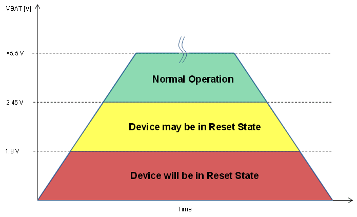
The TAS2552 device has integrated reset circuitry, which requires that VBAT is above 2.45 V for the device to enter normal operation mode. Figure 60 shows the internal thresholds and reset states. Normal operation mode is within the green area of Figure 60.
 Figure 60. VBAT Reset Range
When the supplies have settled, wait at least 1 ms after EN is set HIGH to operate the device. The above sequence should be completed before any I2C operation.
9.3 Boost Supply Details
The boost supply (VBAT) and associated passives need to be able to support the current requirements of the device. By default, the peak current limit of the boost is set to 2.5 A. Please see Configurable Boost Current Limit (ILIM) for information on changing the current limit. A minimum of a 10 µF capacitor is recommended on the boost supply to quickly support changes in required current. Refer to Figure 55 for the schematic.
The current requirements can also be reduced by lowering the gain of the amplifier, or in response to decreasing battery through the use of the battery-tracking AGC feature of the TAS2552 described in Battery Tracking AGC.