SLASE64A December 2014 – June 2017 PCM1860-Q1 , PCM1861-Q1 , PCM1862-Q1 , PCM1863-Q1 , PCM1864-Q1 , PCM1865-Q1
PRODUCTION DATA.
- 1 Features
- 2 Applications
- 3 Description
- 4 Revision History
- 5 Device Comparison Table
- 6 Pin Configuration and Functions
-
7 Specifications
- 7.1 Absolute Maximum Ratings
- 7.2 ESD Ratings
- 7.3 Recommended Operating Conditions
- 7.4 Thermal Information
- 7.5 Electrical Characteristics: PGA and ADC AC Performance
- 7.6 Electrical Characteristics: DC
- 7.7 Electrical Characteristics: Digital Filter
- 7.8 Timing Requirements: External Clock
- 7.9 Timing Requirements: I2C Control Interface
- 7.10 Timing Requirements: SPI Control Interface
- 7.11 Timing Requirements: Audio Data Interface for Slave Mode
- 7.12 Timing Requirements: Audio Data Interface for Master Mode
- 7.13 Typical Characteristics
- 8 Parameter Measurement Information
-
9 Detailed Description
- 9.1 Overview
- 9.2 Functional Block Diagrams
- 9.3
Features Description
- 9.3.1 Analog Front End
- 9.3.2 Microphone Support
- 9.3.3 Input Multiplexer (PCM1860-Q1 and PCM1861-Q1)
- 9.3.4 Mixers and Multiplexers (PCM1862-Q1, PCM1863-Q1, PCM1864-Q1, and PCM1865-Q1)
- 9.3.5 Programmable Gain Amplifier
- 9.3.6 Automatic Clipping Suppression
- 9.3.7 Zero Crossing Detect
- 9.3.8 Digital Inputs
- 9.3.9
Clocks
- 9.3.9.1 Description
- 9.3.9.2 External Clock-Source Limits
- 9.3.9.3 Device Clock Distribution and Generation
- 9.3.9.4
Clocking Modes
- 9.3.9.4.1 Clock Configuration and Selection for Hardware-Controlled Devices
- 9.3.9.4.2 Clock Sources for Software-Controlled Devices
- 9.3.9.4.3 Clocking Configuration and Selection for Software-Controlled Devices
- 9.3.9.4.4 BCK Input Slave PLL Mode
- 9.3.9.4.5 Software-Controlled Devices ADC Non-Audio MCK PLL Mode
- 9.3.9.5 Software-Controlled Devices Manual PLL Calculation
- 9.3.9.6 Clock Halt and Error
- 9.3.9.7 Clock Halt and Error Detect
- 9.3.9.8 Changes in Clock Sources and Sample Rates
- 9.3.10 Analog-to-Digital Converters (ADCs)
- 9.3.11 Energysense
- 9.3.12 Audio Processing
- 9.3.13 Fade-In and Fade-Out Functions
- 9.3.14 Mappable GPIO Pins
- 9.3.15 Interrupt Controller
- 9.3.16 Audio Format Selection and Timing Details
- 9.4 Device Functional Modes
- 9.5 Programming
-
10Application and Implementation
- 10.1 Application Information
- 10.2 Typical Applications
- 11Power Supply Recommendations
- 12Layout
-
13Register Map
- 13.1 Register Map Description
- 13.2 Register Map Summary
- 13.3
Page 0 Registers
- 13.3.1 Page 0: Register 1 (address = 0x01) [reset = 0x00]
- 13.3.2 Page 0: Register 2 (address = 0x02) [reset = 0x00]
- 13.3.3 Page 0: Register 3 (address = 0x03) [reset = 0x00]
- 13.3.4 Page 0: Register 4 (address = 0x04) [reset = 0x00]
- 13.3.5 Page 0: Register 5 (address = 0x05) [reset = 0x86]
- 13.3.6 Page 0: Register 6 (address = 0x06) [reset = 0x41]
- 13.3.7 Page 0: Register 7 (address = 0x07) [reset = 0x41]
- 13.3.8 Page 0: Register 8 (address = 0x08) [reset = 0x42]
- 13.3.9 Page 0: Register 9 (address = 0x09) [reset = 0x42]
- 13.3.10 Page 0: Register 10 (address = 0x0A) [reset = 0x00]
- 13.3.11 Page 0: Register 11 (address = 0x0B) [reset = 0x44]
- 13.3.12 Page 0: Register 12 (address = 0x0C) [reset = 0x00]
- 13.3.13 Page 0: Register 13 (address = 0x0D) [reset = 0x00]
- 13.3.14 Page 0: Register 14 (address = 0x0E) [reset = 0x00]
- 13.3.15 Page 0: Register 15 (address = 0x0F) [reset = 0x00]
- 13.3.16 Page 0: Register 16 (address = 0x10) [reset = 0x01]
- 13.3.17 Page 0: Register 17 (address = 0x11) [reset = 0x20]
- 13.3.18 Page 0: Register 18 (address = 0x12) [reset = 0x00]
- 13.3.19 Page 0: Register 19 (address = 0x13) [reset = 0x00]
- 13.3.20 Page 0: Register 20 (address = 0x14) [reset = 0x00]
- 13.3.21 Page 0: Register 21 (address = 0x15) [reset = 0x00]
- 13.3.22 Page 0: Register 22 (address = 0x16) [reset = 0x00]
- 13.3.23 Page 0: Register 23 (address = 0x17) [reset = 0x00]
- 13.3.24 Page 0: Register 24 (address = 0x18) [reset = 0x00]
- 13.3.25 Page 0: Register 25 (address = 0x19) [reset = 0x00]
- 13.3.26 Page 0: Register 26 (address = 0x1A) [reset = 0x00]
- 13.3.27 Page 0: Register 27 (address = 0x1B) [reset = 0x00]
- 13.3.28 Page 0: Register 32 (address = 0x20) [reset = 0x01]
- 13.3.29 Page 0: Register 33 (address = 0x21) [reset = 0x00]
- 13.3.30 Page 0: Register 34 (address = 0x22) [reset = 0x01]
- 13.3.31 Page 0: Register 35 (address = 0x23) [reset = 0x03]
- 13.3.32 Page 0: Register 37 (address = 0x25) [reset = 0x07]
- 13.3.33 Page 0: Register 38 (address = 0x26) [reset = 0x03]
- 13.3.34 Page 0: Register 39 (address = 0x27) [reset = 0x3F]
- 13.3.35 Page 0: Register 40 (address = 0x28) [reset = 0x01]
- 13.3.36 Page 0: Register 41 (address = 0x29) [reset = 0x00]
- 13.3.37 Page 0: Register 42 (address = 0x2A) [reset = 0x00]
- 13.3.38 Page 0: Register 43 (address = 0x2B) [reset = 0x01]
- 13.3.39 Page 0: Register 44 (address = 0x2C) [reset = 0x00]
- 13.3.40 Page 0: Register 45 (address = 0x2D) [reset = 0x00]
- 13.3.41 Page 0: Register 48 (address = 0x30) [reset = 0x00]
- 13.3.42 Page 0: Register 49 (address = 0x31) [reset = 0x00]
- 13.3.43 Page 0: Register 50 (address = 0x32) [reset = 0x00]
- 13.3.44 Page 0: Register 51 (address = 0x33) [reset = 0x00]
- 13.3.45 Page 0: Register 52 (address = 0x34) [reset = 0x00]
- 13.3.46 Page 0: Register 54 (address = 0x36) [reset = 0x01]
- 13.3.47 Page 0: Register 64 (address = 0x40) [reset =0x80]
- 13.3.48 Page 0: Register 65 (address = 0x41) [reset = 0x7F]
- 13.3.49 Page 0: Register 66 (address = 0x42) [reset = 0x00]
- 13.3.50 Page 0: Register 67 (address = 0x43) [reset = 0x80]
- 13.3.51 Page 0: Register 68 (address = 0x44) [reset = 0x7F]
- 13.3.52 Page 0: Register 69 (address = 0x45) [reset = 0x00]
- 13.3.53 Page 0: Register 70 (address = 0x46) [reset = 0x80]
- 13.3.54 Page 0: Register 71 (address = 0x47) [reset = 0x7F]
- 13.3.55 Page 0: Register 72 (address = 0x48) [reset = 0x00]
- 13.3.56 Page 0: Register 73 (address = 0x49) [reset = 0x80]
- 13.3.57 Page 0: Register 74 (address = 0x4A) [reset = 0x7F]
- 13.3.58 Page 0: Register 75 (address = 0x4B) [reset = 0x00]
- 13.3.59 Page 0: Register 76 (address = 0x4C) [reset = 0x80]
- 13.3.60 Page 0: Register 77 (address = 0x4D) [reset = 0x7F]
- 13.3.61 Page 0: Register 78 (address = 0x4E) [reset = 0x00]
- 13.3.62 Page 0: Register 79 (address = 0x4F) [reset = 0x80]
- 13.3.63 Page 0: Register 80 (address = 0x50) [reset = 0x7F]
- 13.3.64 Page 0: Register 81 (address = 0x51) [reset = 0x00]
- 13.3.65 Page 0: Register 82 (address = 0x52) [reset = 0x80]
- 13.3.66 Page 0: Register 83 (address = 0x53) [reset = 0x7F]
- 13.3.67 Page 0: Register 84 (address = 0x54) [reset = 0x00]
- 13.3.68 Page 0: Register 85 (address = 0x55) [reset = 0x80]
- 13.3.69 Page 0: Register 86 (address = 0x56) [reset = 0x7F]
- 13.3.70 Page 0: Register 87 (address = 0x57) [reset = 0x00]
- 13.3.71 Page 0: Register 88 (address = 0x58) [reset = 0x00]
- 13.3.72 Page 0: Register 89 (address = 0x59) [reset = 0x00]
- 13.3.73 Page 0: Register 90 (address = 0x5A) [reset = 0x00]
- 13.3.74 Page 0: Register 96 (address = 0x60) [reset = 0x01]
- 13.3.75 Page 0: Register 97 (address = 0x61) [reset = 0x00]
- 13.3.76 Page 0: Register 98 (address = 0x62) [reset =0x10]
- 13.3.77 Page 0: Register 112 (address = 0x70) [reset = 0x70]
- 13.3.78 Page 0: Register 113 (address = 0x71) [reset = 0x10]
- 13.3.79 Page 0: Register 114 (address = 0x72) [reset = 0x00]
- 13.3.80 Page 0: Register 115 (address = 0x73) [reset = 0x00]
- 13.3.81 Page 0: Register 116 (address = 0x74) [reset = 0x00]
- 13.3.82 Page 0: Register 117 (address = 0x75) [reset = 0x00]
- 13.3.83 Page 0: Register 120 (address = 0x78) [reset = 0x00]
- 13.4
Page 1 Registers
- 13.4.1 Page 1: Register 1 (address = 0x01) [reset = 0x00]
- 13.4.2 Page 1: Register 2 (address = 0x02) [reset = 0x00]
- 13.4.3 Page 1: Register 4 (address = 0x04) [reset = 0x00]
- 13.4.4 Page 1: Register 5 (address = 0x05) [reset = 0x00]
- 13.4.5 Page 1: Register 6 (address = 0x06) [reset = 0x00]
- 13.4.6 Page 1: Register 7 (address = 0x07) [reset = 0x00]
- 13.4.7 Page 1: Register 8 (address = 0x08) [reset = 0x00]
- 13.4.8 Page 1: Register 9 (address = 0x09) [reset = 0x00]
- 13.4.9 Page 1: Register 10 (address = 0x0A) [reset = 0x00]
- 13.4.10 Page 1: Register 11 (address = 0x0B) [reset = 0x00]
- 13.5 Page 3 Registers
- 13.6 Page 253 Registers
- 14Device and Documentation Support
- 15Mechanical, Packaging, and Orderable Information
12 Layout
12.1 Layout Guidelines
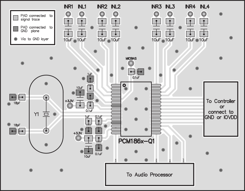
Employ best design practices when laying out a printed circuit board (PCB) for both analog and digital components. The PCM186x-Q1 audio ADC is a relatively simple device to lay out, even on a two-layer PCB. The following basic recommendations for layout of the PCM186x-Q1 help achieve the best possible performance of the device.
- Separate analog and digital sections where layout permits. Route analog lines away from digital lines. This routing technique prevents digital noise from coupling back into analog signals.
- The bottom copper plane can be a shared ground, whereas a ground plane can be used on the top layer as well. Separated planes for analog and digital grounds are not required to achieve data sheet performance.
- Place decoupling capacitors as close as possible to the supply pins, and in the same layer of the device, to yield the best results. Do not place vias between decoupling capacitors and the device.
- Place ground planes between the input traces to achieve the lowest crosstalk performance.
The EVM user’s guide shows the schematics, a bill of material, and a more detailed PCB layout.
12.1.1 Grounding and System Partitioning
Use the same plane for analog and digital grounds to avoid any potential voltage difference between these grounds. On the PCM186x-Q1 EVM, maximum SNR performance is achieved by using a single ground plane, and making sure that the return currents for digital signals are not near the AGND pin or the input signals.
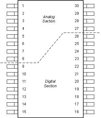
As shown in Figure 74, the pin layout of the PCM186x-Q1 is partitioned into two sections: analog and digital. No digital return currents (for example, clocks) are generated in the analog circuitry, as long as the system is partitioned in such a way that digital signals are routed away from the analog sections.
 Figure 74. Single Ground With Analog Pins Partitioned to the Top and Digital Pins at the Bottom
