SLASEB7D June 2017 – December 2020 MSP430FR6035 , MSP430FR6037 , MSP430FR60371 , MSP430FR6045 , MSP430FR6047 , MSP430FR60471
PRODUCTION DATA
- 1 Features
- 2 Applications
- 3 Description
- 4 Functional Block Diagrams
- 5 Revision History
- 6 Device Comparison
- 7 Terminal Configuration and Functions
-
8 Specifications
- 8.1 Absolute Maximum Ratings
- 8.2 ESD Ratings
- 8.3 Recommended Operating Conditions
- 8.4 Active Mode Supply Current Into VCC Excluding External Current
- 8.5 Typical Characteristics, Active Mode Supply Currents
- 8.6 Low-Power Mode (LPM0, LPM1) Supply Currents Into VCC Excluding External Current
- 8.7 Low-Power Mode (LPM2, LPM3, LPM4) Supply Currents (Into VCC) Excluding External Current
- 8.8 Low-Power Mode With LCD Supply Currents (Into VCC) Excluding External Current
- 8.9 Low-Power Mode (LPMx.5) Supply Currents (Into VCC) Excluding External Current
- 8.10 Typical Characteristics, Low-Power Mode Supply Currents
- 8.11 Typical Characteristics, Current Consumption per Module (1)
- 8.12 Thermal Resistance Characteristics for 100-Pin LQFP (PZ) Package
- 8.13
Timing and Switching Characteristics
- 8.13.1 Power Supply Sequencing
- 8.13.2 Reset Timing
- 8.13.3 Clock Specifications
- 8.13.4 Wake-up Characteristics
- 8.13.5 Digital I/Os
- 8.13.6 LEA
- 8.13.7 Timer_A and Timer_B
- 8.13.8
eUSCI
- 8.13.8.1 eUSCI (UART Mode) Clock Frequency
- 8.13.8.2 eUSCI (UART Mode) Switching Characteristics
- 8.13.8.3 eUSCI (SPI Master Mode) Clock Frequency
- 8.13.8.4 eUSCI (SPI Master Mode) Switching Characteristics
- 8.13.8.5 eUSCI (SPI Master Mode) Timing Diagrams
- 8.13.8.6 eUSCI (SPI Slave Mode) Switching Characteristics
- 8.13.8.7 eUSCI (SPI Slave Mode) Timing Diagrams
- 8.13.8.8 eUSCI (I2C Mode) Switching Characteristics
- 8.13.8.9 eUSCI (SPI Slave Mode) Timing Diagrams
- 8.13.9 Segment LCD Controller
- 8.13.10
ADC12_B
- 8.13.10.1 12-Bit ADC, Power Supply and Input Range Conditions
- 8.13.10.2 12-Bit ADC, Timing Parameters
- 8.13.10.3 12-Bit ADC, Linearity Parameters
- 8.13.10.4 12-Bit ADC, Dynamic Performance With External Reference
- 8.13.10.5 12-Bit ADC, Dynamic Performance With Internal Reference
- 8.13.10.6 12-Bit ADC, Temperature Sensor and Built-In V1/2
- 8.13.10.7 12-Bit ADC, External Reference
- 8.13.10.8 Temperature Sensor Typical Characteristics
- 8.13.11 Reference
- 8.13.12 Comparator
- 8.13.13 FRAM
- 8.13.14 USS
- 8.13.15 Emulation and Debug
-
9 Detailed Description
- 9.1 Overview
- 9.2 CPU
- 9.3 Ultrasonic Sensing Solution (USS) Module
- 9.4 Low-Energy Accelerator (LEA) for Signal Processing
- 9.5 Operating Modes
- 9.6 Interrupt Vector Table and Signatures
- 9.7 Bootloader (BSL)
- 9.8 JTAG Operation
- 9.9 FRAM Controller A (FRCTL_A)
- 9.10 RAM
- 9.11 Tiny RAM
- 9.12 Memory Protection Unit (MPU) Including IP Encapsulation
- 9.13
Peripherals
- 9.13.1 Digital I/O
- 9.13.2 Oscillator and Clock System (CS)
- 9.13.3 Power-Management Module (PMM)
- 9.13.4 Hardware Multiplier (MPY)
- 9.13.5 Real-Time Clock (RTC_C)
- 9.13.6 Measurement Test Interface (MTIF)
- 9.13.7 Watchdog Timer (WDT_A)
- 9.13.8 System Module (SYS)
- 9.13.9 DMA Controller
- 9.13.10 Enhanced Universal Serial Communication Interface (eUSCI)
- 9.13.11 TA0, TA1, and TA4
- 9.13.12 TA2 and TA3
- 9.13.13 TB0
- 9.13.14 ADC12_B
- 9.13.15 USS
- 9.13.16 Comparator_E
- 9.13.17 CRC16
- 9.13.18 CRC32
- 9.13.19 AES256 Accelerator
- 9.13.20 True Random Seed
- 9.13.21 Shared Reference (REF)
- 9.13.22 LCD_C
- 9.13.23 Embedded Emulation
- 9.14
Input/Output Diagrams
- 9.14.1 Port Function Select Registers (PySEL1 , PySEL0)
- 9.14.2 Port P1 (P1.0 and P1.1) Input/Output With Schmitt Trigger
- 9.14.3 Port P1 (P1.2 to P1.7) Input/Output With Schmitt Trigger
- 9.14.4 Port P2 (P2.0 to P2.3) Input/Output With Schmitt Trigger
- 9.14.5 Port P2 (P2.4 to P2.7) Input/Output With Schmitt Trigger
- 9.14.6 Port P3 (P3.0 to P3.7) Input/Output With Schmitt Trigger
- 9.14.7 Port P4 (P4.0 to P4.7) Input/Output With Schmitt Trigger
- 9.14.8 Port P5 (P5.0 to P5.7) Input/Output With Schmitt Trigger
- 9.14.9 Port P6 (P6.0) Input/Output With Schmitt Trigger
- 9.14.10 Port P6 (P6.1 to P6.5) Input/Output With Schmitt Trigger
- 9.14.11 Port P6 (P6.6 and P6.7) Input/Output With Schmitt Trigger
- 9.14.12 Port P7 (P7.0 to P7.3) Input/Output With Schmitt Trigger
- 9.14.13 Port P7 (P7.4) Input/Output With Schmitt Trigger
- 9.14.14 Port P7 (P7.5) Input/Output With Schmitt Trigger
- 9.14.15 Port P7 (P7.6 and P7.7) Input/Output With Schmitt Trigger
- 9.14.16 Port P8 (P8.0 to P8.3) Input/Output With Schmitt Trigger
- 9.14.17 Port P8 (P8.4 to P8.7) Input/Output With Schmitt Trigger
- 9.14.18 Port P9 (P9.0 to P9.3) Input/Output With Schmitt Trigger
- 9.14.19 Port PJ (PJ.0 to PJ.3) JTAG Pins TDO, TMS, TCK, TDI/TCLK, Input/Output With Schmitt Trigger
- 9.14.20 Port PJ (PJ.4 and PJ.5) Input/Output With Schmitt Trigger
- 9.14.21 Port PJ (PJ.6 and PJ.7) Input/Output With Schmitt Trigger
- 9.15 Device Descriptors (TLV)
- 9.16 Memory Map
- 9.17 Identification
-
10Applications, Implementation, and Layout
- 10.1
Device Connection and Layout Fundamentals
- 10.1.1 Power Supply Decoupling and Bulk Capacitors
- 10.1.2 External Oscillator (HFXT and LFXT)
- 10.1.3 USS Oscillator (USSXT)
- 10.1.4 Transducer Connection to the USS Module
- 10.1.5 Charge Pump Control of Input Multiplexer
- 10.1.6 JTAG
- 10.1.7 Reset
- 10.1.8 Unused Pins
- 10.1.9 General Layout Recommendations
- 10.1.10 Do's and Don'ts
- 10.2 Peripheral- and Interface-Specific Design Information
- 10.1
Device Connection and Layout Fundamentals
- 11Device and Documentation Support
- 12Mechanical, Packaging, and Orderable Information
10.1.6 JTAG
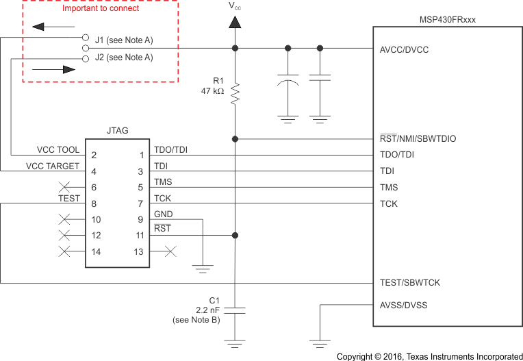
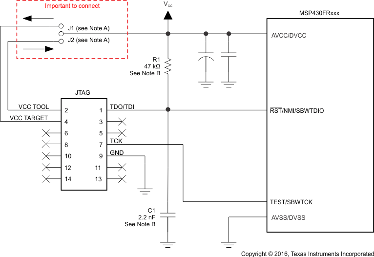
With the proper connections, the debugger and a hardware JTAG interface (such as the MSP-FET or MSP-FET430UIF) can be used to program and debug code on the target board. In addition, the connections also support the MSP-GANG production programmers, thus providing an easy way to program prototype boards, if desired. Figure 10-8 shows the connections between the 14-pin JTAG connector and the target device required to support in-system programming and debugging for 4-wire JTAG communication. Figure 10-9 shows the connections for 2-wire JTAG mode (Spy-Bi-Wire).
The connections for the MSP-FET and MSP-FET430UIF interface modules and the MSP-GANG are identical. Both can supply VCC to the target board (through pin 2). In addition, the MSP-FET and MSP-FET430UIF interface modules and MSP-GANG have a VCC sense feature that, if used, requires an alternate connection (pin 4 instead of pin 2). The VCC sense feature senses the local VCC present on the target board (that is, a battery or other local power supply) and adjusts the output signals accordingly. Figure 10-8 and Figure 10-9 show a jumper block that supports both scenarios of supplying VCC to the target board. If this flexibility is not required, the desired VCC connections may be hard-wired to eliminate the jumper block. Pins 2 and 4 must not be connected at the same time.
For additional design information regarding the JTAG interface, see the MSP430 Hardware Tools User’s Guide.

