SLAU320AJ July   2010  – May 2021


  1.   Trademarks
  2. 1Introduction
    1. 1.1 About This Document
    2. 1.2 Organization of This Document
  3. 2Programming Using the JTAG Interface
    1. 2.1 Introduction
      1. 2.1.1 MSP430 JTAG Restrictions (Noncompliance With IEEE Std 1149.1)
      2. 2.1.2 TAP Controller State Machine
    2. 2.2 Interface and Instructions
      1. 2.2.1 JTAG Interface Signals
        1. 2.2.1.1 Pros and Cons of 2-Wire Spy-Bi-Wire and 4-Wire JTAG
        2. 2.2.1.2 4-Wire JTAG Interface
        3. 2.2.1.3 2-Wire Spy-Bi-Wire (SBW) JTAG Interface
      2. 2.2.2 JTAG Access Macros
        1. 2.2.2.1 Macros for 4-Wire JTAG Interface
          1. 2.2.2.1.1 IR_SHIFT (8-Bit Instruction)
          2. 2.2.2.1.2 DR_SHIFT16 (16-Bit Data)
          3. 2.2.2.1.3 DR_SHIFT20 (20-Bit Address) (Applies Only to MSP430X Devices)
          4. 2.2.2.1.4 MsDelay (Time)
          5. 2.2.2.1.5 SetTCLK
          6. 2.2.2.1.6 ClrTCLK
        2. 2.2.2.2 Macros for Spy-Bi-Wire (SBW) Interface
      3. 2.2.3 Spy-Bi-Wire (SBW) Timing and Control
        1. 2.2.3.1 Basic Timing
        2. 2.2.3.2 TMS Slot
          1. 2.2.3.2.1 TMSH Macro
          2. 2.2.3.2.2 TMSL Macro
          3. 2.2.3.2.3 TMSLDH Macro
        3. 2.2.3.3 TDI Slot
          1. 2.2.3.3.1 TDIH Macro
          2. 2.2.3.3.2 TDIL Macro
        4. 2.2.3.4 TDO Slot
          1. 2.2.3.4.1 TDO_RD Macro
          2. 2.2.3.4.2 TDOsbw Macro (No Read)
        5. 2.2.3.5 TCLK Handling in Spy-Bi-Wire (SBW) Mode
          1. 2.2.3.5.1 SetTCLK and ClrTCLK
          2. 2.2.3.5.2 TCLK Strobes
      4. 2.2.4 JTAG Communication Instructions
        1. 2.2.4.1 Controlling the Memory Address Bus (MAB)
          1. 2.2.4.1.1 IR_ADDR_16BIT
          2. 2.2.4.1.2 IR_ADDR_CAPTURE
        2. 2.2.4.2 Controlling the Memory Data Bus (MDB)
          1. 2.2.4.2.1 IR_DATA_TO_ADDR
          2. 2.2.4.2.2 IR_DATA_16BIT
          3. 2.2.4.2.3 IR_DATA_QUICK
          4. 2.2.4.2.4 IR_BYPASS
        3. 2.2.4.3 Controlling the CPU
          1. 2.2.4.3.1 IR_CNTRL_SIG_16BIT
          2. 2.2.4.3.2 IR_CNTRL_SIG_CAPTURE
          3. 2.2.4.3.3 IR_CNTRL_SIG_RELEASE
        4. 2.2.4.4 Memory Verification by Pseudo Signature Analysis (PSA)
          1. 2.2.4.4.1 IR_DATA_PSA
          2. 2.2.4.4.2 IR_SHIFT_OUT_PSA
        5. 2.2.4.5 JTAG Access Security Fuse Programming
          1. 2.2.4.5.1 IR_PREPARE_BLOW
          2. 2.2.4.5.2 IR_EX_BLOW
    3. 2.3 Memory Programming Control Sequences
      1. 2.3.1 Start-Up
        1. 2.3.1.1 Enable JTAG Access
        2. 2.3.1.2 Fuse Check and Reset of the JTAG State Machine (TAP Controller)
      2. 2.3.2 General Device (CPU) Control Functions
        1. 2.3.2.1 Function Reference for 1xx, 2xx, 4xx Families
          1. 2.3.2.1.1 Taking the CPU Under JTAG Control
          2. 2.3.2.1.2 Set CPU to Instruction-Fetch
          3. 2.3.2.1.3 Setting the Target CPU Program Counter (PC)
          4. 2.3.2.1.4 Controlled Stop or Start of the Target CPU
          5. 2.3.2.1.5 Resetting the CPU While Under JTAG Control
          6. 2.3.2.1.6 Release Device From JTAG Control
        2. 2.3.2.2 Function Reference for 5xx and 6xx Families
          1. 2.3.2.2.1 Taking the CPU Under JTAG Control
          2. 2.3.2.2.2 Setting the Target CPU Program Counter (PC)
          3. 2.3.2.2.3 Resetting the CPU While Under JTAG Control
          4. 2.3.2.2.4 Release Device From JTAG Control
          5. 2.3.2.2.5 74
      3. 2.3.3 Accessing Non-Flash Memory Locations With JTAG
        1. 2.3.3.1 Read Access
        2. 2.3.3.2 Write Access
        3. 2.3.3.3 Quick Access of Memory Arrays
          1. 2.3.3.3.1 Flow for Quick Read (All Memory Locations)
          2. 2.3.3.3.2 Flow for Quick Write
      4. 2.3.4 Programming the Flash Memory (Using the Onboard Flash Controller)
        1. 2.3.4.1 Function Reference for 1xx, 2xx, 4xx Families
        2. 2.3.4.2 Function Reference for 5xx and 6xx Families
      5. 2.3.5 Erasing the Flash Memory (Using the Onboard Flash Controller)
        1. 2.3.5.1 Function Reference for 1xx, 2xx, 4xx Families
          1. 2.3.5.1.1 Flow to Erase a Flash Memory Segment
          2. 2.3.5.1.2 Flow to Erase the Entire Flash Address Space (Mass Erase)
        2. 2.3.5.2 Function Reference for 5xx and 6xx Families
      6. 2.3.6 Reading From Flash Memory
      7. 2.3.7 Verifying the Target Memory
      8. 2.3.8 FRAM Memory Technology
        1. 2.3.8.1 Writing and Reading FRAM
        2. 2.3.8.2 Erasing FRAM
    4. 2.4 JTAG Access Protection
      1. 2.4.1 Burning the JTAG Fuse - Function Reference for 1xx, 2xx, 4xx Families
        1. 2.4.1.1 Standard 4-Wire JTAG
          1. 2.4.1.1.1 Fuse-Programming Voltage on TDI Pin (Dedicated JTAG Pin Devices Only)
          2. 2.4.1.1.2 Fuse-Programming Voltage On TEST Pin
        2. 2.4.1.2 Fuse-Programming Voltage Using SBW
      2. 2.4.2 Programming the JTAG Lock Key - Function Reference for 5xx, 6xx, and FRxx Families
        1. 2.4.2.1 Flash Memory Devices
        2. 2.4.2.2 FRAM Memory Devices
      3. 2.4.3 Testing for a Successfully Protected Device
      4. 2.4.4 Unlocking an FRAM Device in Protected and Secured Modes
        1. 2.4.4.1 FR5xx and FR6xx Devices
        2. 2.4.4.2 FR4xx and FR2xx Devices
      5. 2.4.5 Memory Protection Unit Handling
      6. 2.4.6 Intellectual Property Encapsulation (IPE)
      7. 2.4.7 FRAM Write Protection
    5. 2.5 JTAG Function Prototypes
      1. 2.5.1 Low-Level JTAG Functions
      2. 2.5.2 High-Level JTAG Routines
    6. 2.6 JTAG Features Across Device Families
    7. 2.7 References
  4. 3JTAG Programming Hardware and Software Implementation
    1. 3.1 Implementation History
    2. 3.2 Implementation Overview
    3. 3.3 Software Operation
    4. 3.4 Software Structure
      1. 3.4.1 Programmer Firmware
      2. 3.4.2 Target Code
        1. 3.4.2.1 Target Code Download for Replicator430, Replicator430X, and Replicator430Xv2
        2. 3.4.2.2 Target Code Download for Replicator430FR (FRAM)
    5. 3.5 Hardware Setup
      1. 3.5.1 Host Controller
      2. 3.5.2 Target Connection
      3. 3.5.3 Host Controller or Programmer Power Supply
      4. 3.5.4 Third-Party Support
  5. 4Errata and Revision Information
    1. 4.1 Known Issues
    2. 4.2 Revisions and Errata From Previous Documents
  6. 5Revision History

Enable JTAG Access

This step is only required for devices in which JTAG pins are shared with port I/Os, which is indicated by the presence of a TEST pin. This is the case on all devices that support the Spy-Bi-Wire protocol. Furthermore, some older device groups require special handling to enable 4-wire JTAG (see the "TEST Pin" column in Table 2-14).

Reference function: GetDevice, GetDevice_sbw, GetDevice_430X, GetDevice_430Xv2

  • MSP430 devices with TEST pin and 4-wire JTAG access only (no SBW)

    To use the JTAG features of MSP430 devices with shared JTAG and a TEST pin, it is necessary to enable the shared JTAG pins for JTAG communication mode. Devices with dedicated JTAG inputs/outputs and no TEST pin do not require this step. The shared pins are enabled for JTAG communication by connecting the TEST pin to VCC. For normal operation (non-JTAG mode), this pin should be released, so that it is pulled to ground by the internal pulldown. Table 2-8 shows the port 1 pins that are used for JTAG communication.

    Table 2-8 Shared JTAG Device Pin Functions
    Port 1 Function
    (TEST = Open)
    JTAG Function
    (TEST = VCC)
    P1.4TCK
    P1.5TMS
    P1.6TDI/TCLK
    P1.7TDO
  • MSP430 devices with Spy-Bi-Wire (SBW) access

    The SBW interface and any access to the JTAG interface is disabled while the TEST/SBWTCK pin is held low. This is accomplished by an internal pulldown resistor. The pin can also be tied low externally.

    Pulling the TEST/SBWTCK pin high enables the SBW interface and disables the RST/NMI functionality of the RST/NMI/SBWTDIO pin. While the SBW interface is active, the internal reset signal is held high, and the internal NMI signal is held at the input value seen at RST/NMI with TEST/SBWTCK going high.

    Devices with SBW also support the standard 4-wire interface. The 4-wire JTAG interface access is enabled by pulling the SBWTDIO line low and then applying a clock on SBWTCK. Exit the 4-wire JTAG mode by holding the TEST/SBWTCK low for more than 100 µs.

    To select the 2-wire SBW mode, the SBWTDIO line is held high and the first clock is applied on SBWTCK. After this clock, the normal SBW timings are applied starting with the TMS slot, and the normal JTAG patterns can be applied, typically starting with the Tap Reset and Fuse Check sequence. Exit the SBW mode by holding the TEST/SBWTCK low for more than 100 µs.

    In devices implementing the bootloader (BSL), the TEST/SBWTCK and RST/NMI/SBWTDIO are also used to invoke the BSL. Figure 2-13 shows different cases that are used to enter the SBW/JTAG or BSL mode.
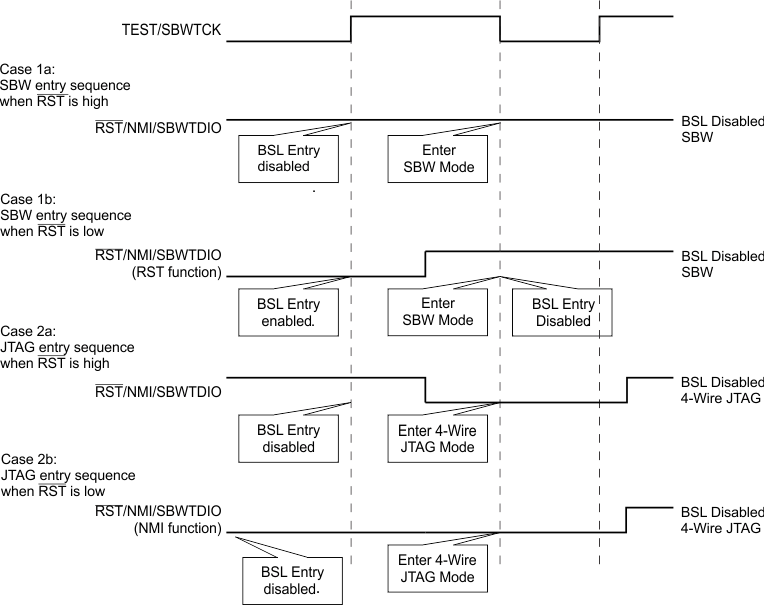
GUID-3672FBA4-FFF1-46BB-8337-912B3E0495B0-low.gifFigure 2-13 JTAG Access Entry Sequences (for Devices That Support SBW)
Note:

On some Spy-Bi-Wire capable MSP430 devices, TEST/SBWTCK is very sensitive to rising signal edges that can cause the test logic to enter a state where an entry sequence (either 2-wire or 4-wire) is not recognized correctly and JTAG access stays disabled. Unintentional edges on SBWTCK can occur when the JTAG connector is connected to the target device. There are two possibilities to work around this problem and ensure a stable JTAG access initialization:

  • Actively drive SBWTCK low before powering up the device or while plugging in the connector to avoid unintentional rising signal edges.
  • Run the initialization sequence multiple times (two to three repeats are typically sufficient to establish a stable connection).