SLAU367P October 2012 – April 2020 MSP430FR5041 , MSP430FR5043 , MSP430FR50431 , MSP430FR5847 , MSP430FR58471 , MSP430FR5848 , MSP430FR5849 , MSP430FR5857 , MSP430FR5858 , MSP430FR5859 , MSP430FR5867 , MSP430FR58671 , MSP430FR5868 , MSP430FR5869 , MSP430FR5870 , MSP430FR5872 , MSP430FR58721 , MSP430FR5887 , MSP430FR5888 , MSP430FR5889 , MSP430FR58891 , MSP430FR5922 , MSP430FR59221 , MSP430FR5947 , MSP430FR59471 , MSP430FR5948 , MSP430FR5949 , MSP430FR5957 , MSP430FR5958 , MSP430FR5959 , MSP430FR5962 , MSP430FR5964 , MSP430FR5967 , MSP430FR5968 , MSP430FR5969 , MSP430FR5969-SP , MSP430FR59691 , MSP430FR5970 , MSP430FR5972 , MSP430FR59721 , MSP430FR5986 , MSP430FR5987 , MSP430FR5988 , MSP430FR5989 , MSP430FR5989-EP , MSP430FR59891 , MSP430FR5992 , MSP430FR5994 , MSP430FR59941 , MSP430FR6005 , MSP430FR6007 , MSP430FR6035 , MSP430FR6037 , MSP430FR60371 , MSP430FR6041 , MSP430FR6043 , MSP430FR60431 , MSP430FR6045 , MSP430FR6047 , MSP430FR60471 , MSP430FR6820 , MSP430FR6822 , MSP430FR68221 , MSP430FR6870 , MSP430FR6872 , MSP430FR68721 , MSP430FR6877 , MSP430FR6879 , MSP430FR68791 , MSP430FR6887 , MSP430FR6888 , MSP430FR6889 , MSP430FR68891 , MSP430FR6920 , MSP430FR6922 , MSP430FR69221 , MSP430FR6927 , MSP430FR69271 , MSP430FR6928 , MSP430FR6970 , MSP430FR6972 , MSP430FR69721 , MSP430FR6977 , MSP430FR6979 , MSP430FR69791 , MSP430FR6987 , MSP430FR6988 , MSP430FR6989 , MSP430FR69891
4.4.2.1 MSP430 Instruction With Indexed Mode in Lower 64KB Memory
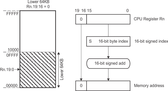
If the CPU register Rn points to an address in the lower 64KB of the memory range, the calculated memory address bits 19:16 are cleared after the addition of the CPU register Rn and the signed 16-bit index. This means the calculated memory address is always located in the lower 64KB and does not overflow or underflow out of the lower 64KB memory space. The RAM and the peripheral registers can be accessed this way and existing MSP430 software is usable without modifications as shown in Figure 4-15.
 Figure 4-15 Indexed Mode in Lower 64KB
 | Length: | 2 or 3 words |
| Operation: | The signed 16-bit index is located in the next word after the instruction and is added to the CPU register Rn. The resulting bits 19:16 are cleared giving a truncated 16-bit memory address, which points to an operand address in the range 00000h to 0FFFFh. The operand is the content of the addressed memory location. |
| Comment: | Valid for source and destination. The assembler calculates the register index and inserts it. |
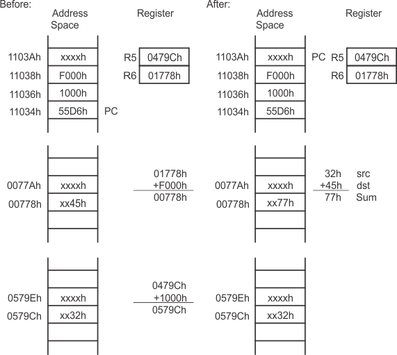
| Example: | ADD.B 1000h(R5),0F000h(R6); |
| This instruction adds the 8-bit data contained in source byte 1000h(R5) and the destination byte 0F000h(R6) and places the result into the destination byte. Source and destination bytes are both located in the lower 64KB due to the cleared bits 19:16 of registers R5 and R6. | |
| Source: | The byte pointed to by R5 + 1000h results in address 0479Ch + 1000h = 0579Ch after truncation to a 16-bit address. |
| Destination: | The byte pointed to by R6 + F000h results in address 01778h + F000h = 00778h after truncation to a 16-bit address. |
