SLLA525A October 2020 – April 2021 TCAN1043-Q1 , TCAN1043G-Q1 , TCAN1043H-Q1 , TCAN1043HG-Q1
4 Pin Failure Mode Analysis (Pin FMA)
This section provides a Failure Mode Analysis (FMA) for the pins of the TCAN1043-Q1 (as well as the TCAN1043G-Q1, TCAN1043H-Q1, and TCAN1043HG-Q1). The failure modes covered in this document include the typical pin-by-pin failure scenarios:
- Pin short-circuited to Ground (see Table 4-2)
- Pin open-circuited (see Table 4-3)
- Pin short-circuited to an adjacent pin (see Table 4-4)
- Pin short-circuited to VSUP (see Table 4-5)
- Pin short-circuited to VCC (see Table 4-6)
- Pin short-circuited to VIO (see Table 4-7)
Table 4-2 through Table 4-7 also indicate how these pin conditions can affect the device as per the failure effects classification in Table 4-1.
| Class | Failure Effects |
|---|---|
| A | Potential device damage that affects functionality |
| B | No device damage, but loss of functionality |
| C | No device damage, but performance degradation |
| D | No device damage, no impact to functionality or performance |
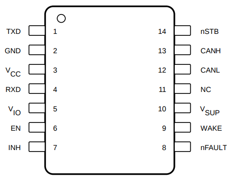
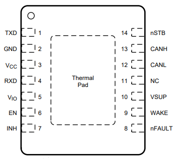
Figure 4-1 shows the TCAN1043-Q1 SOIC pin diagram. Figure 4-2 shows the TCAN1043-Q1 VSON pin diagram. For a detailed description of the device pins please refer to the Pin Configuration and Functions section in the TCAN1043-Q1 data sheet.
 Figure 4-1 TCAN1043-Q1 SOIC Pin
Diagram
 Figure 4-2 TCAN1043-Q1 VSON Pin
Diagram
Figure 4-2 TCAN1043-Q1 VSON Pin
DiagramFollowing are the assumptions of use and the device configuration assumed for the pin FMA in this section:
- VCC = 4.5 V to 5.5 V
- VSUP = 4.5 V to 45 V (4.5 to 60 V for the H-version)
- VIO = 2.8 V to 5.5 V
| Pin Name | Pin No. | Description of Potential Failure Effect(s) | Failure Effect Class |
|---|---|---|---|
| TXD | 1 | TXD will be biased dominant indefinitely and device will enter dominant time out mode. Unable to transmit data. | B |
| GND | 2 | None | D |
| VCC | 3 | Device will be in protected mode, high current draw from external regulator supplying VCC. | B |
| RXD | 4 | Receiver output biased recessive indefinitely. Host unable to receive data from bus. | B |
| VIO | 5 | Device will be in protected mode. Transceiver passive on bus, and high current draw from external regulator supplying VIO. | B |
| EN | 6 | EN pin biased low, device will not be able to enter normal mode. Unable to communicate. | B |
| INH | 7 | High ISUP current, INH pin may be damaged and indication from sleep mode transition not available. | A |
| nFAULT | 8 | nFAULT pin biased low indefinitely which indicates a fault indefinitely. | B |
| WAKE | 9 | WAKE pin biased low indefinitely, will not be able to utilize local wake-up function. | B |
| VSUP | 10 | Device unpowered, high ISUP current. | B |
| NC | 11 | None | D |
| CANL | 12 | VO(REC) spec violated. Degraded EMC performance. | C |
| CANH | 13 | Device cannot drive dominant to the bus, no communication possible. | B |
| nSTB | 14 | nSTB biased low indefinitely, transceiver unable to enter normal mode. Unable to communicate. | B |
| Thermal Pad | - | None | D |
| Pin Name | Pin No. | Description of Potential Failure Effect(s) | Failure Effect Class |
|---|---|---|---|
| TXD | 1 | TXD pin defaults to a recessive bias, device is always recessive and unable to transmit data. | B |
| GND | 2 | Device unpowered. | B |
| VCC | 3 | Device in protected mode. | B |
| RXD | 4 | No RXD output, unable to receive data. | B |
| VIO | 5 | Device in protected mode. | B |
| EN | 6 | EN pin defaults to a logic-low bias, device will not be able to enter normal mode. Unable to communicate. | B |
| INH | 7 | None | D |
| nFAULT | 8 | No effect on performance, unable to monitor system faults. | B |
| WAKE | 9 | No effect on device performance, will not be able to utilize local wake-up function. | B |
| VSUP | 10 | Device unpowered. | B |
| NC | 11 | None | D |
| CANL | 12 | Device cannot drive dominant on bus, unable to communicate. | B |
| CANH | 13 | Device cannot drive dominant on bus, unable to communicate. | B |
| nSTB | 14 | nSTB defaults to a logic-low bias, device will not be able to enter normal mode. Unable to communicate. | B |
| Thermal Pad | - | None | D |
| Pin Name | Pin No. | Shorted to | Description of Potential Failure Effect(s) | Failure Effect Class |
|---|---|---|---|---|
| TXD | 1 | GND | TXD will be biased dominant indefinitely and device will enter dominant time out mode. Unable to transmit data. | B |
| GND | 2 | VCC | Device will be in protected mode, high ICC current. | B |
| VCC | 3 | RXD | RXD output biased recessive indefinitely, controller unable to receive data from CAN bus. | B |
| RXD | 4 | VIO | RXD output biased recessive indefinitely, controller unable to receive data from CAN bus. | B |
| VIO | 5 | EN | EN pin biased high indefinitely, device will be unable to enter standby and silent mode. | B |
| EN | 6 | INH | Absolute maximum violation on EN pin except in sleep mode. Transceiver may be damaged. | A |
| nFAULT | 8 | WAKE | Potential absolute maximum violation on nFAULT pin if WAKE is biased high. Transceiver may be damaged. | A |
| WAKE | 9 | VSUP | WAKE biased high indefinitely, unable to utilize local wake-up function. | B |
| VSUP | 10 | NC | None | D |
| NC | 11 | CANL | None | D |
| CANL | 12 | CANH | Bus biased recessive, no communication possible. IOS current may be reached on CANH/CANL. | B |
| CANH | 13 | nSTB | Driver and receiver turn off when the CAN bus is recessive. May not enter normal mode. | B |
| Pin Name | Pin No. | Description of Potential Failure Effect(s) | Failure Effect Class |
|---|---|---|---|
| TXD | 1 | Absolute maximum violation, transceiver may be damaged. | A |
| GND | 2 | Device unpowered, high ISUP current. | B |
| VCC | 3 | Absolute maximum violation, transceiver may be damaged. | A |
| RXD | 4 | Absolute maximum violation, transceiver may be damaged. | A |
| VIO | 5 | Absolute maximum violation, transceiver may be damaged. | A |
| EN | 6 | Absolute maximum violation, transceiver may be damaged. | A |
| INH | 7 | Minimal current driven into the INH pin. | D |
| nFAULT | 8 | Absolute maximum violation, transceiver may be damaged. | A |
| WAKE | 9 | WAKE biased high, unable to utilize local wake-up function. | B |
| VSUP | 10 | None | D |
| NC | 11 | None | D |
| CANL | 12 | IOS current may be reached. RXD always recessive. | B |
| CANH | 13 | VO(REC) spec violated, degraded EMC performance and communcation errors may result as well. | C |
| nSTB | 14 | Absolute maximum violation, transceiver may be damaged. | A |
| Pin Name | Pin No. | Description of Potential Failure Effect(s) | Failure Effect Class |
|---|---|---|---|
| TXD | 1 | TXD biased recessive indefinitely, unable to transmit data. | B |
| GND | 2 | Device unpowered, high current draw from external regulator supplying VCC. | B |
| VCC | 3 | None | D |
| RXD | 4 | Receiver output biased recessive indefinitely. Host unable to receive data from bus. | B |
| VIO | 5 | IO pins will operate as 5V input/outputs. Microcontroller may be damaged if VCC > VIO. | C |
| EN | 6 | EN biased high indefinitely, device will be unable to enter standby and silent mode. | B |
| INH | 7 | Absolute maximum violation on VCC pin, INH will be biased at VCC voltage, system may not wake up. | B |
| nFAULT | 8 | nFAULT biased high indefinitely, transceiver unable to report faults. | B |
| WAKE | 9 | None | D |
| VSUP | 10 | Absolute maximum violation on VCC. | B |
| NC | 11 | None | D |
| CANL | 12 | IOS current may be reached, RXD always recessive. | B |
| CANH | 13 | VO(REC) spec violated, degraded EMC performance. | C |
| nSTB | 14 | nSTB biased high indefinitely, transceiver unable to enter standby and sleep mode. | B |
| Pin Name | Pin No. | Description of Potential Failure Effect(s) | Failure Effect Class |
|---|---|---|---|
| TXD | 1 | TXD biased recessive indefinitely, unable to transmit data. | B |
| GND | 2 | Device unpowered, high current draw from external regulator supplying VIO. | B |
| VCC | 3 | IO pins will operate as 5V input/outputs. Microcontroller may be damaged if VCC > VIO. | C |
| RXD | 4 | Receiver output biased recessive indefinitely. Host unable to receive data from bus. | B |
| VIO | 5 | None | D |
| EN | 6 | EN biased high indefinitelyf, device will be unable to enter standby and silent mode. | B |
| INH | 7 | Absolute maximum violation on VIO pin, INH will be biased at VIO voltage, system may not wake up. | B |
| nFAULT | 8 | nFAULT biased high indefinitely, transceiver unable to report faults. | B |
| WAKE | 9 | None | D |
| VSUP | 10 | Absolute maximum violation on VIO. | B |
| NC | 11 | None | D |
| CANL | 12 | IOS current may be reached, RXD always recessive. | B |
| CANH | 13 | VO(REC) spec violated, degraded EMC performance. | C |
| nSTB | 14 | nSTB biased high indefinitely, transceiver unable to enter standby and sleep mode. | B |