SLLA639 May 2024 THVD1419 , THVD1429 , THVD1439 , THVD1449 , THVD2419 , THVD2429
2 Discrete Approach to RS-485 Surge Protection
Most classical RS-485 devices, while robust in the face of many standard industrial environments, still cannot withstand a high voltage surge on the differential communication bus pins without sustaining damage. Many industrial system designers when faced with this problem can employ a discrete protection network, which depending on the on the characteristics of the surge signal the transceiver can be exposed to can vary in complexity. However, before a discussion of common discrete protection circuits are discussed, a way to evaluate the surge signal can be discussed.
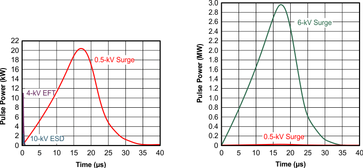
Many designers, when contemplating surge protection, need a way to quickly quantify the amount of surge protection received. A common standard, and the one that TI also evaluates to, is IEC 61000 4-5 which is a common standard that devices such as TVS diodes, gas discharge tubes (GDT), and Metal Oxide Varistors (MOV) use to standardize a parameter for surge immunity. It is typical to test with a 1.2/50 – 8/20us surge generator – where the voltage waveform has a 1.2us rise time and 50us fall time with the current waveform having an 8us rise time followed by a 20us fall time. This standard is what underpins what surge immunity means to many devices, including those from TI. Both a 0.5kV and a 6kV surge showing the power over time are shown in Figure 2-1
 Figure 2-1 Surge and ESD Power Comparison
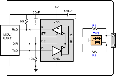
The simplest protection scheme works by limiting current, clamping the line voltage, and additional filtering of the peak surge current coming into the differential line.
 Figure 2-2 RS-485 Half Duplex Transceiver with Basic Discrete Surge Protection
In Figure 2-2 the incoming surge at the port has the current limited to set the clamping voltage of the TVS diode. It is very important to understand what level the diode can clamp the bus to under expected surge conditions – the current shunted through the diode can be directly related to the bus clamping voltage so it is very important to have current limiting between surge source and bus protection. R1 and R2 are low value resistors that are pulse proof – typically the resistors can be thick film or wire wound and sized to about 10Ω. These resistors help filter off the short-lasting peak voltages coming in from the bus which further increases the overall rating of the node. Many TI RS-485 data sheets suggest using the CDSOT23-SM712 diode paired with CRCW0603010RJNEAHP thick film resistors.
| Component | Package Dimensions | Package/Design Area |
|---|---|---|
| CDSOT23-SM712 | 2.9mm x 2.3mm | 6.67mm^2 |
| CRCWO603010RJNEAHP | 1.55mm x 0.85mm | 1.3175mm^2 |
| Standard 8-Pin RS-485 Transceiver in SOIC package | 4.9mm x 3.91mm | 19.16mm^2 |
| Total Design Size: (2 Resistors, 1 IC, 1 diode) | N/A | 28.465mm^2 |
Adding the two resistors and diode necessary for basic surge protection adds almost 50% of the IC package space to the total space budget. This also does not include layout considerations that can also end up increasing the total design size. The aforementioned design is something TI only recommends to about ±1kV surges, but higher surge levels can require larger diodes.
It is important to understand the maximum voltages that can be seen by the transceiver. If the bus clamps too high, the transceiver can still be damaged, so it is critical for the designer to keep track of the clamping voltage of the bus. Beyond size increases and strict voltage maximums of the transceiver this design has one other flaw – the surge voltages must be relatively short lasting. The TVS diodes typically used in RS-485 protection systems cannot sustain high amounts of current being shunted through them indefinitely. Also, if the diodes are left too long under high current conditions the diodes can break and the resulting spike in voltage on the bus can result in a damaged transceiver as well as destroyed protection devices.
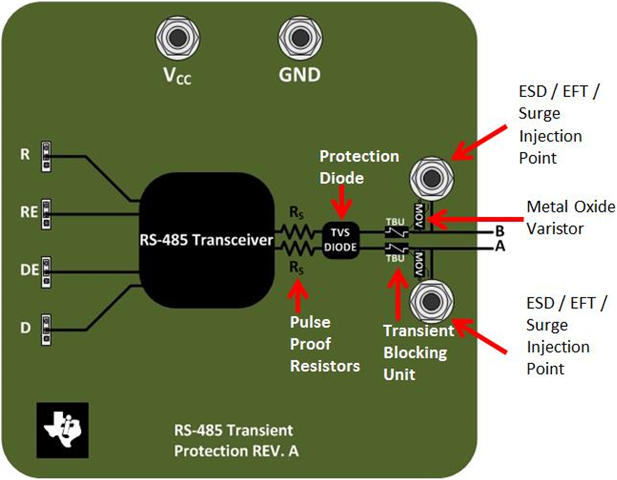
While the simple approach to protection as previously discussed has a lot of benefit to many systems, other systems can require more robust approaches. A tried and true method of achieving even higher levels of protection in the system is to employ Transient Blocking Units (TBUs) and Metal Oxide Varistors (MOV) in addition to the simple network described previously.
 Figure 2-3 Robust Discrete Surge Protection for RS-485 Bus
Figure 2-3 shows that the simple network of TVS diodes and pulse proof resistors still exists in the same position as it can be in a simpler protection scheme. However, the TBUs and MOVs have also been added to increase the robustness. The TBUs are shown as both a current limiter as well as a voltage disconnect circuit. During an overvoltage or overcurrent event, the TBU can limit the current running through the device then after a brief delay can effectively break the load off, including the RS-485 device, from the surge source. The MOVs act similarly to bi-directional surge diodes and additional clamping stage to the bus for protection under large surges. They do not protect against in-rush current and can possible have issues with sustained current faults. Due to these limitations, they are paired with the TBU to help add current protection as well as voltage clamping on the main bus line.
In most surge protected RS-485 systems, either the simple or complex variation can be found, while there can be outliers – these two designs are considered well tested for specific protection needs. However, with each additional element added to the board, the complexity of the design and board space needed increases which can put considerable strain on the designer to adequately meet all of the design goals.