SLLSEY2G March 2017 – August 2021 ISOW7840 , ISOW7841 , ISOW7842 , ISOW7843 , ISOW7844
PRODUCTION DATA
- 1 Features
- 2 Applications
- 3 Description
- 4 Revision History
- 5 Description (continued)
- 6 Pin Configuration and Functions
-
7 Specifications
- 7.1 Absolute Maximum Ratings
- 7.2 ESD Ratings
- 7.3 Recommended Operating Conditions
- 7.4 Thermal Information
- 7.5 Power Ratings
- 7.6 Insulation Specifications
- 7.7 Safety-Related Certifications
- 7.8 Safety Limiting Values
- 7.9 Electrical Characteristics—5-V Input, 5-V Output
- 7.10 Supply Current Characteristics—5-V Input, 5-V Output
- 7.11 Electrical Characteristics—3.3-V Input, 5-V Output
- 7.12 Supply Current Characteristics—3.3-V Input, 5-V Output
- 7.13 Electrical Characteristics—5-V Input, 3.3-V Output
- 7.14 Supply Current Characteristics—5-V Input, 3.3-V Output
- 7.15 Electrical Characteristics—3.3-V Input, 3.3-V Output
- 7.16 Supply Current Characteristics—3.3-V Input, 3.3-V Output
- 7.17 Switching Characteristics—5-V Input, 5-V Output
- 7.18 Switching Characteristics—3.3-V Input, 5-V Output
- 7.19 Switching Characteristics—5-V Input, 3.3-V Output
- 7.20 Switching Characteristics—3.3-V Input, 3.3-V Output
- 7.21 Insulation Characteristics Curves
- 7.22 Typical Characteristics
- 8 Parameter Measurement Information
- 9 Detailed Description
- 10Application and Implementation
- 11Power Supply Recommendations
- 12Layout
- 13Device and Documentation Support
- 14Mechanical, Packaging, and Orderable Information
10.2 Typical Application

|
For step-by-step design procedure, circuit schematics, bill of materials, printed circuit board (PCB) files, simulation results, and test results, refer to TI Design TIDA-01333, Eight-Channel, Isolated, High-Voltage Analog Input Module With ISOW7841 Reference Design. |
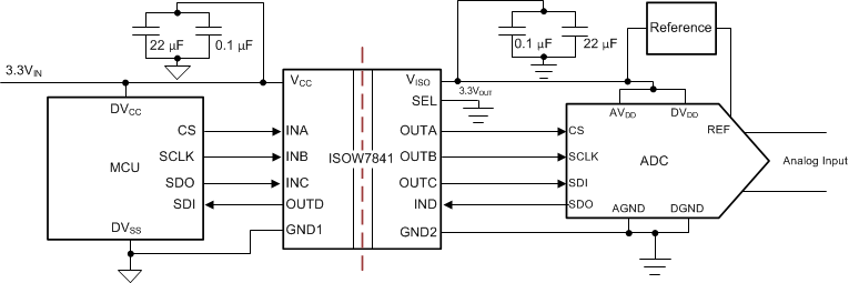
Figure 10-1 shows the typical schematic for SPI isolation.
 Figure 10-1 Isolated
Power and SPI for ADC Sensing Application with ISOW7841