SLLSFA0C July 2019 – May 2024 ISO7021
PRODUCTION DATA
- 1
- 1 Features
- 2 Applications
- 3 Description
- 4 Device Comparison Table
- 5 Pin Configuration and Functions
-
6 Specifications
- 6.1 Absolute Maximum Ratings
- 6.2 ESD Ratings
- 6.3 Recommended Operating Conditions
- 6.4 Thermal Information
- 6.5 Power Ratings
- 6.6 Insulation Specifications
- 6.7 Safety-Related Certifications
- 6.8 Safety Limiting Values
- 6.9 Electrical Characteristics 5V Supply
- 6.10 Supply Current Characteristics 5V Supply
- 6.11 Electrical Characteristics 3.3V Supply
- 6.12 Supply Current Characteristics 3.3V Supply
- 6.13 Electrical Characteristics 2.5V Supply
- 6.14 Supply Current Characteristics 2.5V Supply
- 6.15 Electrical Characteristics 1.8V Supply
- 6.16 Supply Current Characteristics 1.8V Supply
- 6.17 Switching Characteristics
- 7 Parameter Measurement Information
- 8 Detailed Description
- 9 Application and Implementation
- 10Power Supply Recommendations
- 11Layout
- 12Device and Documentation Support
- 13Revision History
- 14Mechanical, Packaging, and Orderable Information
3 Description
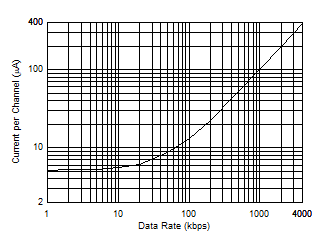
The ISO7021 device is an ultra-low power, multichannel digital isolator that can be used to isolate CMOS or LVCMOS digital I/Os. Each isolation channel has a logic input and output buffer separated by a double capacitive silicon dioxide (SiO2) insulation barrier. Innovative edge based architecture combined with an ON-OFF keying modulation scheme allows these isolators to consume very-low power while meeting 3000VRMS isolation rating per UL1577. The per channel dynamic current consumption of the device is under 120μA/Mbps and the per channel static current consumption is 4.8μA at 3.3V, allowing for use of the ISO7021 in both power and thermal constrained system designs.
The device can operate as low as 1.71V, as high as 5.5V , and is fully functional with different supply voltages on each side of isolation barrier. The two-channel isolator comes in a narrow body 8-SOIC package with one forward and one reverse-direction channel in a 8-SOIC package. The device has default output high and low options. If the input power or signal is lost, default output is high for the ISO7021 device without the suffix F and low for the ISO7021F device with the F suffix. See the Device Functional Modes section for more information.
 Data Rate vs Power Consumption at 3.3V