SLLU166A June 2012 – September 2022 ISO1540 , ISO1540-Q1 , ISO1541 , ISO1541-Q1
1.3 Functional Configuration
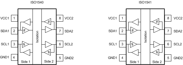
The pinouts of ISO1540 and ISO1541 are displayed in Figure 1-1. These devices have an input noise-filter that prevents transient pulses of up to 5 ns from being passed to the output of the device.
 Figure 1-1 ISO1540 and ISO1541 Pinout
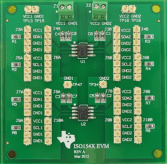
The EVM is shown in Figure 1-2, it comes with an ISO1540 and an ISO1541 installed in place of U1 and U2 respectively. However, this EVM can be configured for use with two ISO1540s or two ISO1541s.
 Figure 1-2 ISO154xEVM Top Photograph
An input or output pin can be tied either to supply voltage (VCCx) or Ground (GNDx) using the 4-pin jumpers on the EVM (J3A to J10A on side 1 and J3B to J10B on side 2). These jumpers also provide scope-probe access to each pin.
Each signal line (SDAx, SCLx) is configured with a 1-kΩ pull-up resistor (R1 to R8) to the corresponding power supply (VCCx). Reconfigure the value of this pull-up resistor as per the application requirement.