SLLU166A June 2012 – September 2022 ISO1540 , ISO1540-Q1 , ISO1541 , ISO1541-Q1
1.4 EVM Schematic
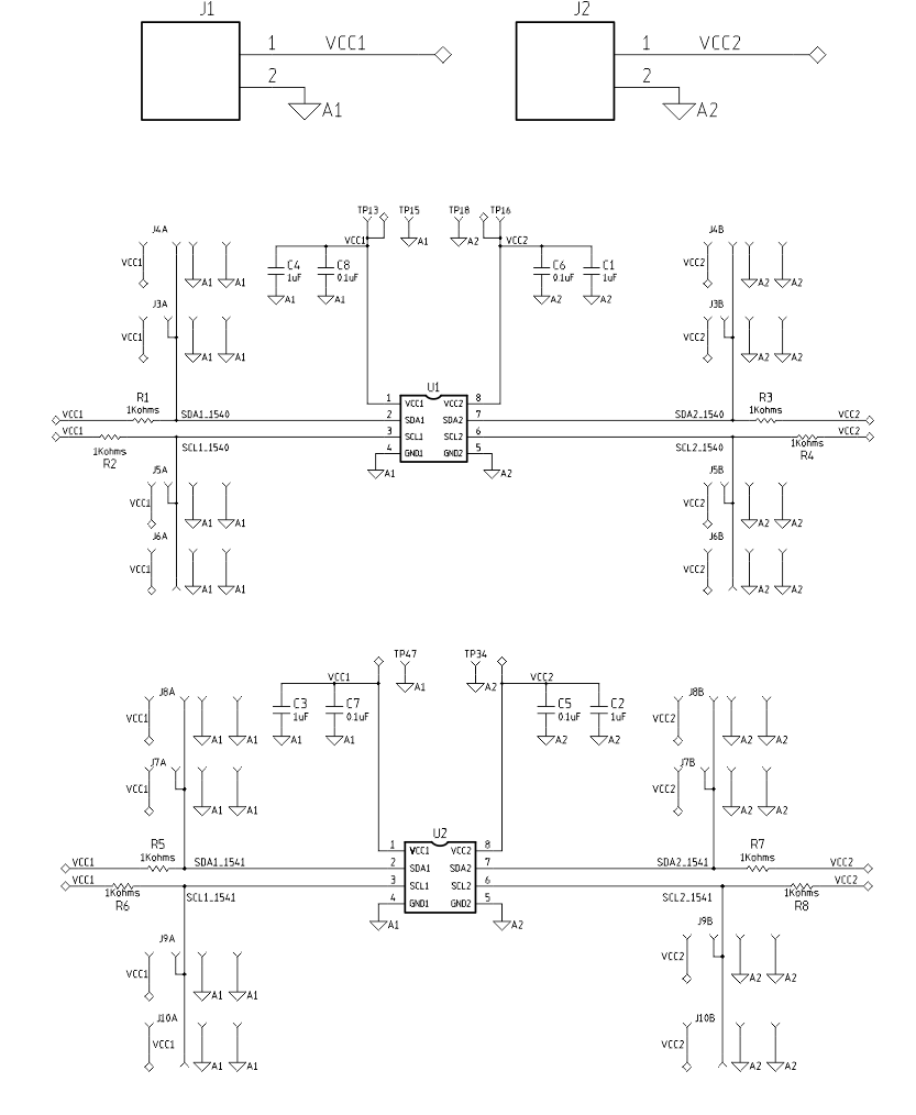
A schematic diagram for this EVM is presented in Figure 1-3.
 Figure 1-3 ISO154xEVM Schematic
Table 1-1 ISO154xEVM Description
| Label | Description |
|---|---|
| U1 | ISO154x, by default populated as ISO1540 |
| U2 | ISO154x, by default populated as ISO1541 |
| J1 | Side 1 power supply terminal block (VCC1) |
| J2 | Side 2 power supply terminal block (VCC2) |
| TP15, TP47 | Side 1 GND test point (GND1) |
| TP18, TP34 | Side 2 GND test point (GND2) |
| TP13 | VCC1 test point |
| TP16 | VCC2 test point |
| J3A, J4A | 4-pin jumper to VCC1, SDA1, GND1 for U1 |
| J5A, J6A | 4-pin jumper to VCC1, SCL1, GND1 for U1 |
| J3B, J4B | 4-pin jumper to VCC2, SDA2, GND2 for U1 |
| J5B, J6B | 4-pin jumper to VCC2, SCL2, GND2 for U1 |
| J7A, J8A | 4-pin jumper to VCC1, SDA1, GND1 for U2 |
| J9A, J10A | 4-pin jumper to VCC1, SCL1, GND1 for U2 |
| J7B, J8B | 4-pin jumper to VCC2, SDA2, GND2 for U2 |
| J9B, J10B | 4-pin jumper to VCC2, SCL2, GND2 for U2 |
| C1, C2, C3, C4 | 1.0 µF filter capacitor |
| C5, C6, C7, C8 | 0.1 µF filter capacitor |
| R1, R2, R5, R6 | 1-kΩ 0603 footprint pull-up resistor to VCC1 |
| R3, R4, R7, R8 | 1-kΩ 0603 footprint pull-up resistor to VCC2 |