SLOA284A january 2020 – may 2023 AFE5832 , AFE5832LP , ISO7741 , ISOW7841 , LM25037 , LM25180 , LM5180 , LM5181 , LM5181-Q1 , TX7316 , TX7332
6 Clock Synchronization
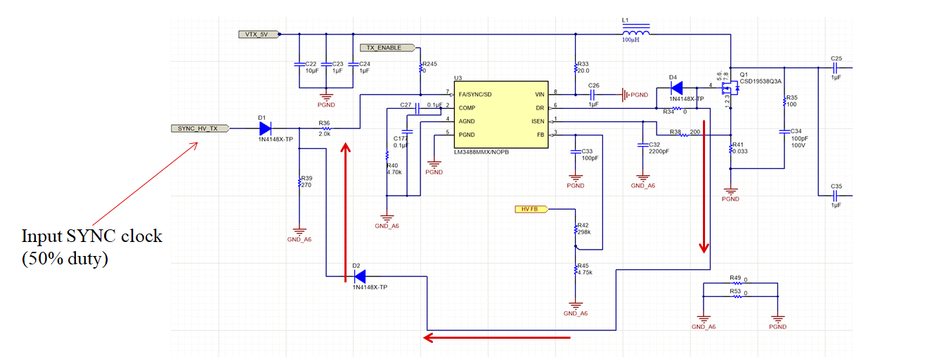
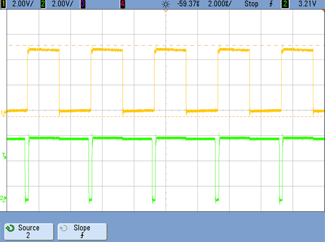
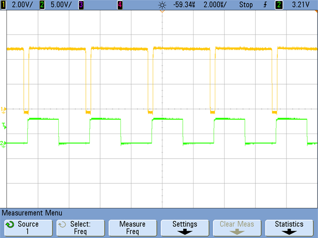
The schematic shown in Figure 2-2 can be synchronized to an external clock signal only if the duty cycle of the latter is larger than the duty cycle of the controller itself (larger than 93%). This design can be synchronized to an external clock with 50% Duty cycle by implementing the solution shown in Figure 6-1. Two diodes forming an OR-ing system are introduced. One diode is placed from the gate drive pin to the sync pin. The other one comes from the input clock signal. The resistor R36 and R39 are series SYNC resistor and discharge resistor, respectively. If DR_pin is more positive than SYNC_HV_TX, then D1 will be reverse-biased and the SYNC-PIN will be driven high from D2. If DR_pin is less positive than SYNC_HV_TX, then D2 will be reverse-biased and SYNC_PIN will be driven High from D1. Test results are shown in Figure 6-2 and Figure 6-3.
 Figure 6-1 Section of the Schematic of HV
Supply Updated After Implementation of SYNC Functionality
 Figure 6-2 Synchronization at No Load
With 50% Duty Cycle Clock
 Figure 6-3 Synchronization at Full
Load With 50% Duty Cycle Clock