SLOA337 October 2024 TAS6584-Q1 , TAS6684-Q1
1 Introduction
There are several existing application notes on determining the proper LC filter for class-D amplifiers, such as LC Filter Design and Inductor Selection Guide for 2.1MHz Class-D Amplifiers, that discuss considerations when determining the output LC filter configuration, inductor values, and capacitor values.
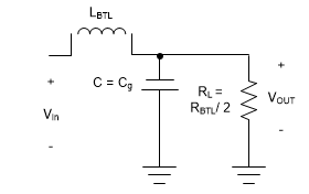
TAS6x84-Q1 is a high-power class-D audio amplifier, supporting up to 45V voltage and at least 10A current per channel, and uses BD or 1SPW mode modulation. Figure 1-1 shows the LC filter single-ended equivalent circuit. BD and 1SPW mode modulation use same LC filter configuration.
 Figure 1-1 LC Filter for BD and 1SPW Mode
(Half is Shown)
Figure 1-1 LC Filter for BD and 1SPW Mode
(Half is Shown)Ripple current on the inductors is defined as the alternating current flowing through the output inductor of a class-D amplifier. With an LC filter, specifically as the cutoff frequency of the LC filter is reduced relative to the PWM switching frequency of the amplifier, the ripple current is reduced such that only a small residual ripple voltage is present after the LC filter. Lower ripple current is also desired in LC filter design to reduce power loss across the RDS(on) of the output FETs and the DCR of the output inductors, and EMC radiation interference.
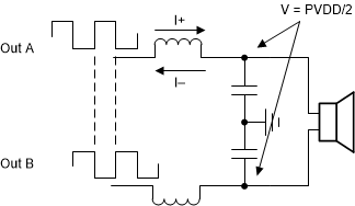
The ripple current contributes the most to the total idle current. Figure 1-2 shows that when in BD modulation mode, class-D amplifiers produce a common-mode voltage of PVDD / 2 after the LC filter at idle, which is the average value of the 50% duty-cycle PWM switching waveform (see Figure 1-3).
 Figure 1-2 PVDD / 2 Common-Mode
Voltage
Figure 1-2 PVDD / 2 Common-Mode
VoltageTherefore, the voltage across the output
inductor changes the polarity when the PWM voltage reaches
PVDD / 2. The maximum voltage across the inductor is PVDD / 2 and the minimum
voltage is –PVDD / 2.
 Figure 1-3 PWM Voltage Waveform
Figure 1-4 shows the inductor voltage and current waveforms drawn using these arguments.
 Figure 1-4 Inductor Voltage and
Current
Figure 1-4 Inductor Voltage and
CurrentAt idle, the positive and negative current flow through the inductor must be symmetrical and therefore centered around zero. Otherwise, there is a DC offset across the speaker and a constant average current flow through the load. The shaded regions in Figure 1-4 indicate the direction of current flow.
Using Figure 1-4, the peak ripple current at idle can be calculated.
where
- L = inductor value
- fPWM = PWM switching frequency
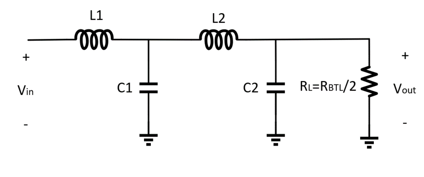
As the power voltage increases, the peak ripple current also increases. Consider increasing the inductance to reduce the output ripple current. On high-voltage applications, use a fourth-order filter configuration for better EMC performance. Figure 1-5 is a typical TAS6x84 LC filter configuration that can cover all voltage applications.
 Figure 1-5 TAS6x84-Q1 Typical LC Filter
Circuit (Half is Shown)